
Datasheet


LTC2050/LTC2050HV
5
2050fc
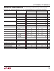
PARAMETER CONDITIONS
C, I SUFFIXES H SUFFIX
UNITSMIN TYP MAX MIN TYP MAX
Input Offset Voltage (Note 2) ±0.5 ±3 ±0.5 ±3 μV
Average Input Offset Drift (Note 2)
l
±0.03 ±0.05 μV/°C
Long-Term Offset Drift 50 50 nV/√mo
Input Bias Current LTC2050
l
±75 ±150
±300
±75 ±150
±4000
pA
pA
LTC2050HV
l
±7 ±50
±150
±7 ±50
±4000
pA
pA
Input Offset Current LTC2050
l
±300
±400
±300
±1000
pA
pA
LTC2050HV
l
±100
±200
±100
±1000
pA
pA
Input Noise Voltage R
S
= 100Ω, 0.01Hz to 10Hz 1.5 1.5 μV
P-P
Common Mode Rejection Ratio V
CM
= GND to (V
+
– 1.3)
V
CM
= GND to (V
+
– 1.3)
l
120
115
130
130
120
110
130
130
dB
dB
Power Supply Rejection Ratio V
S
= 2.7V to 6V
l
120
115
130
130
120
115
130
130
dB
dB
Large-Signal Voltage Gain R
L
= 10k
l
125
120
140
140
125
115
140
140
dB
dB
Output Voltage Swing High R
L
= 2k to GND
R
L
= 10k to GND
l
l
4.85
4.95
4.94
4.98
4.85
4.95
4.94
4.98
V
V
Output Voltage Swing Low R
L
= 2k to GND
R
L
= 10k to GND
l
l
1
1
10
10
1
1
10
10
mV
mV
Slew Rate 22V/μs
Gain Bandwidth Product 3 3 MHz
Supply Current V
SHDN
= V
IH
, No Load
V
SHDN
= V
IL
l
l
0.8 1.2
15
0.8 1.3
15
mA
μA
Shutdown Pin Input Low Voltage (V
IL
)
l
V
–
+ 0.5 V
–
+ 0.5 V
Shutdown Pin Input High Voltage (V
IH
)
l
V
+
– 0.5 V
+
– 0.5 V
Shutdown Pin Input Current V
SHDN
= GND
l
–0.5 –7 –0.5 –7 μA
Internal Sampling Frequency 7.5 7.5 kHz
ELECTRICAL CHARACTERISTICS
The l denotes the specifi cations which apply over the full operating
temperature range, otherwise specifi cations are at T
A
= 25°C. (LTC2050/LTC2050HV) V
S
= 5V unless otherwise noted. (Note 3)