
Datasheet


1
LTC2051/LTC2052
20512fd
Dual/Quad Zero-Drift
Operational Amplifiers
■
Thermocouple Amplifiers
■
Electronic Scales
■
Medical Instrumentation
■
Strain Gauge Amplifiers
■
High Resolution Data Acquisition
■
DC Accurate RC Active Filters
■
Low Side Current Sense
■
Maximum Offset Voltage of 3μV
■
Maximum Offset Voltage Drift of 30nV/°C
■
Small Footprint, Low Profile MS8/GN16 Packages
■
Single Supply Operation: 2.7V to ±5.5V
■
Noise: 1.5μV
P-P
(0.01Hz to 10Hz Typ)
■
Voltage Gain: 140dB (Typ)
■
PSRR: 130dB (Typ)
■
CMRR: 130dB (Typ)
■
Supply Current: 0.75mA (Typ) per Amplifier
■
Extended Common Mode Input Range
■
Output Swings Rail-to-Rail
■
Operating Temperature Range –40°C to 125°C
■
Available in 3mm × 3mm × 0.8mm DFN Package
The LTC
®
2051/LTC2052 are dual/quad zero-drift opera-
tional amplifiers available in the MS8 and SO-8/GN16 and
S14 packages. For space limited applications, the LTC2051
is available in a 3mm × 3mm × 0.8mm dual fine pitch
leadless package (DFN). They operate from a single 2.7V
supply and support ±5V applications. The current con-
sumption is 750μA per op amp.
The LTC2051/LTC2052, despite their miniature size, fea-
ture uncompromising DC performance. The typical input
offset voltage and offset drift are 0.5μV and 10nV/°C. The
almost zero DC offset and drift are supported with a power
supply rejection ratio (PSRR) and common mode rejec-
tion ratio (CMRR) of more than 130dB.
The input common mode voltage ranges from the negative
supply up to typically 1V from the positive supply. The
LTC2051/LTC2052 also have an enhanced output stage
capable of driving loads as low as 2kΩ to both supply rails.
The open-loop gain is typically 140dB. The LTC2051/
LTC2052 also feature a 1.5μV
P-P
DC to 10Hz noise and a
3MHz gain-bandwidth product.
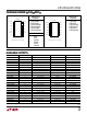
Input Referred Noise 0.1Hz to 10Hz
High Performance Low Cost Instrumentation Amplifier
, LT, LTC and LTM are registered trademarks of Linear Technology Corporation.
All other trademarks are the property of their respective owners.
2
1
0
–1
–2
μV
0246810
TIME (SEC)
2052 TA02
FEATURES
DESCRIPTIO
U
APPLICATIO S
U
TYPICAL APPLICATIO
U
–
+
R2
10k
0.1%
R1
100Ω
0.1%
7
4
5
6
3
2
20512 TA01
–5V
–
+
1/2
LTC2051HV
1/2
LTC2051HV
8
1
5V
–V
IN
V
IN
A
V
= 101
R2
10k
0.1%
R1
100Ω
0.1%