
Datasheet


LTC2053/LTC2053-SYNC
3
2053syncfc
elecTrical characTerisTics
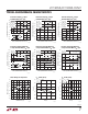
PARAMETER CONDITIONS MIN TYP MAX UNITS
Gain Error A
V
= 1
l
0.001 0.01 %
Gain Nonlinearity A
V
= 1, LTC2053
A
V
= 1, LTC2053-SYNC
l
l
3
3
12
15
ppm
ppm
Input Offset Voltage (Note 2) V
CM
= 200mV –5 ±10 µV
Average Input Offset Drift (Note 2) T
A
= –40°C to 85°C
T
A
= 85°C to 125°C
l
l
–1
±50
–2.5
nV/°C
µV/°C
Average Input Bias Current (Note 3) V
CM
= 1.2V
l
4 10 nA
Average Input Offset Current (Note 3) V
CM
= 1.2V
l
1 3 nA
Input Noise Voltage DC to 10Hz 2.5 µV
P-P
Common Mode Rejection Ratio
(Notes 4, 5)
A
V
= 1, V
CM
= 0V to 3V, LTC2053C, LTC2053C-SYNC
A
V
= 1, V
CM
= 0.1V to 2.9V, LTC2053I, LTC2053I-SYNC
A
V
= 1, V
CM
= 0V to 3V, LTC2053I, LTC2053I-SYNC
A
V
= 1, V
CM
= 0.1V to 2.9V, LTC2053H
A
V
= 1, V
CM
= 0V to 3V, LTC2053H
l
l
l
l
l
100
100
95
100
85
113
113
113
dB
dB
dB
dB
dB
Power Supply Rejection Ratio (Note 6) V
S
= 2.7V to 6V
l
110 116 dB
Output Voltage Swing High R
L
= 2k to V
–
R
L
= 10k to V
–
l
l
2.85
2.95
2.94
2.98
V
V
Output Voltage Swing Low
l
20 mV
Supply Current No Load
l
0.75 1 mA
Supply Current, Shutdown V
EN
≥ 2.5V, LTC2053 Only 10 µA
EN/CLK Pin Input Low Voltage, V
IL
0.5 V
EN/CLK Pin Input High Voltage, V
IH
2.5 V
EN/CLK Pin Input Current V
EN/CLK
= V
–
–0.5 –10 µA
Internal Op Amp Gain Bandwidth 200 kHz
Slew Rate 0.2 V/µs
Internal Sampling Frequency 3 kHz
The l denotes the specifications which apply over the full operating
temperature range, otherwise specifications are at T
A
= 25°C. V
+
= 3V, V
–
= 0V, REF = 200mV. Output voltage swing is referenced
to V
–
. All other specifications reference the OUT pin to the REF pin.
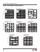
The l denotes the specifications which apply over the full operating temperature range, otherwise specifications are at T
A
= 25°C.
V
+
= 5V, V
–
= 0V, REF = 200mV. Output voltage swing is referenced to V
–
. All other specifications reference the OUT pin to the REF pin.
PARAMETER CONDITIONS MIN TYP MAX UNITS
Gain Error A
V
= 1
l
0.001 0.01 %
Gain Nonlinearity A
V
= 1
l
3 10 ppm
Input Offset Voltage (Note 2) V
CM
= 200mV –5 ±10 µV
Average Input Offset Drift (Note 2) T
A
= –40°C to 85°C
T
A
= 85°C to 125°C
l
l
–1
±50
–2.5
nV/°C
µV/°C
Average Input Bias Current (Note 3) V
CM
= 1.2V
l
4 10 nA
Average Input Offset Current (Note 3) V
CM
= 1.2V
l
1 3 nA
Common Mode Rejection Ratio
(Notes 4, 5)
A
V
= 1, V
CM
= 0V to 5V, LTC2053C
A
V
= 1, V
CM
= 0V to 5V, LTC2053C-SYNC
A
V
= 1, V
CM
= 0.1V to 4.9V, LTC2053I
A
V
= 1, V
CM
= 0.1V to 4.9V, LTC2053I-SYNC
A
V
= 1, V
CM
= 0V to 5V, LTC2053I, LTC2053I-SYNC
A
V
= 1, V
CM
= 0.1V to 4.9V, LTC2053H
A
V
= 1, V
CM
= 0V to 5V, LTC2053H
l
l
l
l
l
l
l
105
100
105
100
95
100
85
116
116
116
116
116
dB
dB
dB
dB
dB
dB
dB
Power Supply Rejection Ratio (Note 6) V
S
= 2.7V to 6V
l
110 116 dB