LTC2142-14/ LTC2141-14/LTC2140-14 14-Bit, 65Msps/ 40Msps/25Msps Low Power Dual ADCs DESCRIPTION FEATURES n n n n n n n n n n n n n The LTC®2142-14/LTC2141-14/LTC2140-14 are 2-channel simultaneous sampling 14-bit A/D converters designed for digitizing high frequency, wide dynamic range signals. They are perfect for demanding communications applications with AC performance that includes 73.2dB SNR and 90dB spurious free dynamic range (SFDR). Ultralow jitter of 0.
LTC2142-14/ LTC2141-14/LTC2140-14 ABSOLUTE MAXIMUM RATINGS (Notes 1, 2) Supply Voltages (VDD, OVDD) ....................... –0.3V to 2V Analog Input Voltage (AIN+, AIN –, PAR/SER, SENSE) (Note 3) .......... –0.3V to (VDD + 0.2V) Digital Input Voltage (ENC+, ENC–, CS, SDI, SCK) (Note 4) .................................... –0.3V to 3.9V SDO (Note 4)............................................. –0.3V to 3.9V Digital Output Voltage ................ –0.3V to (OVDD + 0.
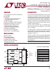
LTC2142-14/ LTC2141-14/LTC2140-14 PIN CONFIGURATIONS DOUBLE DATA RATE LVDS OUTPUT MODE 64 VDD 63 SENSE 62 VREF 61 SDO 60 OF2_1+ 59 OF2_1– 58 D1_12_13+ 57 D1_12_13– 56 D1_10_11+ 55 D1_10_11– 54 D1_8_9+ 53 D1_8_9– 52 D1_6_7+ 51 D1_6_7– 50 D1_4_5+ 49 D1_4_5– TOP VIEW VDD 1 VCM1 2 GND 3 AIN1+ 4 AIN1– 5 GND 6 REFH 7 REFL 8 REFH 9 REFL 10 PAR/SER 11 AIN2+ 12 AIN2– 13 GND 14 VCM2 15 VDD 16 48 D1_2_3+ 47 D1_2_3– 46 D1_0_1+ 45 D1_0_1– 44 DNC 43 DNC 42 OVDD 41 OGND 40 CLKOUT+ 39 CLKOUT– 38 D2_12_13+ 37 D2_12_13–
LTC2142-14/ LTC2141-14/LTC2140-14 CONVERTER CHARACTERISTICS The l denotes the specifications which apply over the full operating temperature range, otherwise specifications are at TA = 25°C. (Note 5) LTC2142-14 PARAMETER CONDITIONS Resolution (No Missing Codes) Integral Linearity Error MIN l LTC2141-14 TYP MAX MIN ±1 2.4 –2.4 14 Differential Analog Input (Note 6) l –2.4 LTC2140-14 TYP MAX MIN ±1 2.4 –2.4 14 TYP MAX UNITS ±1 2.
LTC2142-14/ LTC2141-14/LTC2140-14 DYNAMIC ACCURACY The l denotes the specifications which apply over the full operating temperature range, otherwise specifications are at TA = 25°C. AIN = –1dBFS.
LTC2142-14/ LTC2141-14/LTC2140-14 DIGITAL INPUTS AND OUTPUTS The l denotes the specifications which apply over the full operating temperature range, otherwise specifications are at TA = 25°C. (Note 5) SYMBOL PARAMETER CONDITIONS MIN TYP MAX UNITS ENCODE INPUTS (ENC+, ENC– ) Differential Encode Mode (ENC– Not Tied to GND) VID Differential Input Voltage (Note 8) l 0.2 VICM Common Mode Input Voltage Internally Set Externally Set (Note 8) l 1.1 1.6 V V l 0.2 3.6 V V 1.
LTC2142-14/ LTC2141-14/LTC2140-14 POWER REQUIREMENTS The l denotes the specifications which apply over the full operating temperature range, otherwise specifications are at TA = 25°C. (Note 9) LTC2142-14 SYMBOL PARAMETER CONDITIONS LTC2141-14 LTC2140-14 MIN TYP MAX MIN TYP MAX MIN TYP MAX UNITS CMOS Output Modes: Full Data Rate and Double Data Rate VDD Analog Supply Voltage (Note 10) l 1.7 1.8 1.9 1.7 1.8 1.9 1.7 1.8 1.9 V OVDD Output Supply Voltage (Note 10) l 1.1 1.8 1.
LTC2142-14/ LTC2141-14/LTC2140-14 TIMING CHARACTERISTICS The l denotes the specifications which apply over the full operating temperature range, otherwise specifications are at TA = 25°C. (Note 5) SYMBOL PARAMETER CONDITIONS MIN TYP MAX UNITS Digital Data Outputs (LVDS Mode) tD ENC to Data Delay CL = 5pF (Note 8) l 1.1 1.8 3.2 ns tC ENC to CLKOUT Delay CL = 5pF (Note 8) l 1 1.5 2.7 ns tSKEW DATA to CLKOUT Skew tD – tC (Note 8) l 0 0.3 0.6 ns Pipeline Latency 6.
LTC2142-14/ LTC2141-14/LTC2140-14 TYPICAL PERFORMANCE CHARACTERISTICS LTC2142-14: Differential Nonlinearity (DNL) LTC2142-14: Integral Nonlinearity (INL) 2.0 1.5 1.0 0 0.8 –10 –20 0.6 0.5 0 –0.5 –1.0 –30 0.4 AMPLITUDE (dBFS) DNL ERROR (LSB) 1.0 INL ERROR (LSB) LTC2142-14: 64k Point FFT, fIN = 5MHz, –1dBFS, 65Msps 0.2 0 –0.2 –0.4 –0.8 –2.0 –1.
LTC2142-14/ LTC2141-14/LTC2140-14 TYPICAL PERFORMANCE CHARACTERISTICS LTC2142-14: 2nd, 3rd Harmonic vs Input Frequency, –1dBFS, 65Msps, 1V Range LTC2142-14: 2nd, 3rd Harmonic vs Input Frequency, –1dBFS, 65Msps, 2V Range 100 100 95 95 LTC2142-14: SFDR vs Input Level, fIN = 70MHz, 65Msps, 2V Range 130 90 3RD 85 80 2ND 75 70 65 0 50 100 150 200 250 INPUT FREQUENCY (MHz) 300 3RD 90 85 2ND 80 75 100 90 80 70 dBc 60 50 40 70 65 dBFS 110 SFDR (dBc AND dBFS) 2ND AND 3RD HARMONIC (dBFS) 2ND AN
LTC2142-14/ LTC2141-14/LTC2140-14 TYPICAL PERFORMANCE CHARACTERISTICS 0 0 –10 –10 –20 –20 –20 –30 –30 –30 –40 –50 –60 –70 –80 –90 –100 AMPLITUDE (dBFS) 0 –10 AMPLITUDE (dBFS) AMPLITUDE (dBFS) LTC2141-14: 64k Point FFT, fIN = 140MHz, –1dBFS, 40Msps LTC2141-14: 64k Point FFT, fIN = 70MHz, –1dBFS, 40Msps LTC2141-14: 64k Point FFT, fIN = 30MHz, –1dBFS, 40Msps –40 –50 –60 –70 –80 –90 0 5 10 15 FREQUENCY (MHz) –80 –110 –120 5 21421014 G19 LTC2141-14: 64k Point 2-Tone FFT, fIN = 69MHz, 7
LTC2142-14/ LTC2141-14/LTC2140-14 TYPICAL PERFORMANCE CHARACTERISTICS LTC2141-14: IVDD vs Sample Rate, 5MHz, –1dBFS, Sine Wave Input on Each Channel LTC2141-14: IOVDD vs Sample Rate, 5MHz, –1dBFS, Sine Wave Input on Each Channel 45 70 74 3.5mA LVDS 60 40 73 72 50 35 40 71 SNR (dBFS) LVDS OUTPUTS IOVDD (mA) IVDD (mA) LTC2141-14: SNR vs SENSE, fIN = 5MHz, –1dBFS 1.75mA LVDS 30 70 69 CMOS OUTPUTS 20 30 68 10 67 1.
LTC2142-14/ LTC2141-14/LTC2140-14 TYPICAL PERFORMANCE CHARACTERISTICS LTC2140-14: 64k Point 2-Tone FFT, fIN = 69MHz, 70MHz, –7dBFS, 25Msps LTC2140-14: SNR vs Input Frequency, –1dBFS, 25Msps, 2V Range LTC2140-14: Shorted Input Histogram 6000 0 74 –10 5000 –20 –30 DIFFERENTIAL ENCODE –50 –60 SNR (dBFS) 4000 –40 COUNT AMPLITUDE (dBFS) SINGLE-ENDED ENCODE 73 3000 –70 –80 2000 –90 –100 1000 –110 –120 5 FREQUENCY (MHz) 8183 10 8185 21421014 G37 LTC2140-14: 2nd, 3rd Harmonic vs Input Frequ
LTC2142-14/ LTC2141-14/LTC2140-14 PIN FUNCTIONS PINS THAT ARE THE SAME FOR ALL DIGITAL OUTPUT MODES VDD (Pins 1, 16, 17, 64): Analog Power Supply, 1.7V to 1.9V. Bypass to ground with 0.1μF ceramic capacitors. Adjacent pins can share a bypass capacitor. VCM1 (Pin 2): Common Mode Bias Output, Nominally Equal to VDD/2. VCM1 should be used to bias the common mode of the analog inputs to channel 1. Bypass to ground with a 0.1μF ceramic capacitor. GND (Pins 3, 6, 14): ADC Power Ground.
LTC2142-14/ LTC2141-14/LTC2140-14 PIN FUNCTIONS SENSE (Pin 63): Reference Programming Pin. Connecting SENSE to VDD selects the internal reference and a ±1V input range. Connecting SENSE to ground selects the internal reference and a ±0.5V input range. An external reference between 0.625V and 1.3V applied to SENSE selects an input range of ±0.8 • VSENSE. Ground (Exposed Pad Pin 65): The exposed pad must be soldered to the PCB ground.
LTC2142-14/ LTC2141-14/LTC2140-14 PIN FUNCTIONS D1_0_1–/D1_0_1+ to D1_12_13–/D1_12_13+ (Pins 45/46, 47/48, 49/50, 51/52, 53/54, 55/56, 57/58): Channel 1 Double Data Rate Digital Outputs. Two data bits are multiplexed onto each differential output pair. The even data bits (D0, D2, D4, D6, D8, D10, D12) appear when CLKOUT+ is low. The odd data bits (D1, D3, D5, D7, D9, D11, D13) appear when CLKOUT+ is high. OF2_1–/OF2_1+ (Pins 59/60): Over/Underflow Digital Output.
LTC2142-14/ LTC2141-14/LTC2140-14 TIMING DIAGRAMS Full Rate CMOS Output Mode Timing All Outputs Are Single-Ended and Have CMOS Levels tAP CH 1 ANALOG INPUT A+3 tAP CH 2 ANALOG INPUT A+4 A+2 A A+1 B+4 B+2 B B+3 tH B+1 tL ENC– ENC+ tD D1_0 - D1_13, OF1 A–6 A–5 A–4 A–3 A–2 D2_0 - D2_13, OF2 B–6 B–5 B–4 B–3 B–2 CLKOUT + CLKOUT – tC 21421014 TD01 21421014fa 17
LTC2142-14/ LTC2141-14/LTC2140-14 TIMING DIAGRAMS Double Data Rate CMOS Output Mode Timing All Outputs Are Single-Ended and Have CMOS Levels tAP CH 1 ANALOG INPUT A+3 tAP CH 2 ANALOG INPUT A+4 A+2 A A+1 B+4 B+2 B B+3 tH B+1 tL ENC– ENC+ tD tD BIT 0 A-6 BIT 1 A-6 BIT 0 A-5 BIT 1 A-5 BIT 0 A-4 BIT 1 A-4 BIT 0 A-3 BIT 1 A-3 BIT 0 A-2 D1_12_13 BIT 12 A-6 BIT 13 A-6 BIT 12 A-5 BIT 13 A-5 BIT 12 A-4 BIT 13 A-4 BIT 12 A-3 BIT 13 A-3 BIT 12 A-2 D2_0_1 BIT 0 B-6 BIT 1 B-6 BIT 0 B-5
LTC2142-14/ LTC2141-14/LTC2140-14 TIMING DIAGRAMS Double Data Rate LVDS Output Mode Timing All Outputs Are Differential and Have LVDS Levels tAP CH 1 ANALOG INPUT A+4 A+2 A A+3 tAP CH 2 ANALOG INPUT A+1 B+4 B+2 B B+3 tH B+1 tL ENC– ENC+ tD D1_0_1+ D1_0_1– tD BIT 0 A-6 BIT 1 A-6 BIT 0 A-5 BIT 1 A-5 BIT 0 A-4 BIT 1 A-4 BIT 0 A-3 BIT 1 A-3 BIT 0 A-2 BIT 12 A-6 BIT 13 A-6 BIT 12 A-5 BIT 13 A-5 BIT 12 A-4 BIT 13 A-4 BIT 12 A-3 BIT 13 A-3 BIT 12 A-2 BIT 0 B-6 BIT 1 B-6 BIT 0 B-5
LTC2142-14/ LTC2141-14/LTC2140-14 APPLICATIONS INFORMATION CONVERTER OPERATION The LTC2142-14/LTC2141-14/LTC2140-14 are low power, 2-channel, 14-bit, 65Msps/40Msps/25Msps A/D converters that are powered by a single 1.8V supply. The analog inputs should be driven differentially. The encode input can be driven differentially, or single ended for lower power consumption.
LTC2142-14/ LTC2141-14/LTC2140-14 APPLICATIONS INFORMATION Amplifier Circuits Reference Figure 7 shows the analog input being driven by a high speed differential amplifier. The output of the amplifier is ACcoupled to the A/D so the amplifier’s output common mode voltage can be optimally set to minimize distortion. The LTC2142-14/LTC2141-14/LTC2140-14 has an internal 1.25V voltage reference. For a 2V input range using the internal reference, connect SENSE to VDD.
LTC2142-14/ LTC2141-14/LTC2140-14 APPLICATIONS INFORMATION REFL pins are connected by short jumpers in an internal layer. To minimize the inductance of these jumpers they can be placed in a small hole in the GND plane on the second board layer. LTC2142 VREF 1.25V 5Ω 1.25V BANDGAP REFERENCE 2.2μF 0.625V TIE TO VDD FOR 2V RANGE; TIE TO GND FOR 1V RANGE; 3"/(& t 7SENSE FOR 0.625V < VSENSE < 1.300V RANGE DETECT AND CONTROL SENSE BUFFER INTERNAL ADC HIGH REFERENCE C2 0.1μF – + + – REFL 0.
LTC2142-14/ LTC2141-14/LTC2140-14 APPLICATIONS INFORMATION LTC2142 ENC– should stay at least 200mV above ground to avoid falsely triggering the single ended encode mode. For good jitter performance ENC+ and ENC– should have fast rise and fall times. VDD DIFFERENTIAL COMPARATOR VDD 15k ENC+ ENC– 30k 21421014 F10 Figure 10. Equivalent Encode Input Circuit for Differential Encode Mode If the encode signal is turned off or drops below approximately 500kHz, the A/D enters nap mode. LTC2142 1.8V TO 3.
LTC2142-14/ LTC2141-14/LTC2140-14 APPLICATIONS INFORMATION Full Rate CMOS Mode In full rate CMOS mode the data outputs (D1_0 to D1_13 and D2_0 to D2_13), overflow (OF2, OF1), and the data output clocks (CLKOUT+, CLKOUT–) have CMOS output levels. The outputs are powered by OVDD and OGND which are isolated from the A/D core power and ground. OVDD can range from 1.1V to 1.9V, allowing 1.2V through 1.8V CMOS logic outputs. For good performance, the digital outputs should drive minimal capacitive loads.
LTC2142-14/ LTC2141-14/LTC2140-14 APPLICATIONS INFORMATION Phase Shifting the Output Clock DATA FORMAT In full rate CMOS mode the data output bits normally change at the same time as the falling edge of CLKOUT+, so the rising edge of CLKOUT+ can be used to latch the output data. In double data rate CMOS and LVDS modes the data output bits normally change at the same time as the falling and rising edges of CLKOUT+.
LTC2142-14/ LTC2141-14/LTC2140-14 APPLICATIONS INFORMATION Digital Output Randomizer CLKOUT Interference from the A/D digital outputs is sometimes unavoidable. Digital interference may be from capacitive or inductive coupling or coupling through the ground plane. Even a tiny coupling factor can cause unwanted tones in the ADC output spectrum. By randomizing the digital output before it is transmitted off chip, these unwanted tones can be randomized which reduces the unwanted tone amplitude.
LTC2142-14/ LTC2141-14/LTC2140-14 APPLICATIONS INFORMATION Digital Output Test Patterns To allow in-circuit testing of the digital interface to the A/D, there are several test modes that force the A/D data outputs (OF, D13-D0) to known values: All 1s: All outputs are 1 All 0s: All outputs are 0 Alternating: Outputs change from all 1s to all 0s on alternating samples. Checkerboard: Outputs change from 101010101010101 to 010101010101010 on alternating samples.
LTC2142-14/ LTC2141-14/LTC2140-14 APPLICATIONS INFORMATION Serial Programming Mode GROUNDING AND BYPASSING To use the serial programming mode, PAR/SER should be tied to ground. The CS, SCK, SDI and SDO pins become a serial interface that program the A/D mode control registers. Data is written to a register with a 16-bit serial word. Data can also be read back from a register to verify its contents. The LTC2142-14/LTC2141-14/LTC2140-14 requires a printed circuit board with a clean unbroken ground plane.
LTC2142-14/ LTC2141-14/LTC2140-14 APPLICATIONS INFORMATION Table 3. Serial Programming Mode Register Map (PAR/SER = GND) REGISTER A0: RESET REGISTER (ADDRESS 00h) D7 D6 D5 D4 D3 D2 D1 D0 RESET X X X X X X X Bit 7 RESET Software Reset Bit 0 = Not Used 1 = Software Reset. All Mode Control Registers Are Reset to 00h. The ADC Is Momentarily Placed in SLEEP Mode. This Bit Is Automatically Set Back to Zero at the end of the SPI write command. The Reset Register Is Write-only.
LTC2142-14/ LTC2141-14/LTC2140-14 APPLICATIONS INFORMATION REGISTER A3: OUTPUT MODE REGISTER (ADDRESS 03h) D7 D6 D5 D4 D3 D2 D1 D0 X ILVDS2 ILVDS1 ILVDS0 TERMON OUTOFF OUTMODE1 OUTMODE0 Bit 7 Unused, Don’t Care Bit. Bits 6-4 ILVDS2:ILVDS0 LVDS Output Current Bits 000 = 3.5mA LVDS Output Driver Current 001 = 4.0mA LVDS Output Driver Current 010 = 4.5mA LVDS Output Driver Current 011 = Not Used 100 = 3.0mA LVDS Output Driver Current 101 = 2.5mA LVDS Output Driver Current 110 = 2.
LTC2142-14/ LTC2141-14/LTC2140-14 TYPICAL APPLICATIONS Silkscreen Top Top Side 21421014fa 31
LTC2142-14/ LTC2141-14/LTC2140-14 TYPICAL APPLICATIONS Inner Layer 2 GND Inner Layer 3 21421014fa 32
LTC2142-14/ LTC2141-14/LTC2140-14 TYPICAL APPLICATIONS Inner Layer 4 Inner Layer 5 Power 21421014fa 33
LTC2142-14/ LTC2141-14/LTC2140-14 TYPICAL APPLICATIONS Bottom Side 21421014fa 34
LTC2142-14/ LTC2141-14/LTC2140-14 TYPICAL APPLICATIONS SDO C23 2.
LTC2142-14/ LTC2141-14/LTC2140-14 PACKAGE DESCRIPTION UP Package 64-Lead Plastic QFN (9mm w 9mm) (Reference LTC DWG # 05-08-1705 Rev C) 0.70 ±0.05 7.15 ±0.05 7.50 REF 8.10 ±0.05 9.50 ±0.05 (4 SIDES) 7.15 ±0.05 PACKAGE OUTLINE 0.25 ±0.05 0.50 BSC RECOMMENDED SOLDER PAD PITCH AND DIMENSIONS APPLY SOLDER MASK TO AREAS THAT ARE NOT SOLDERED 9 .00 ±0.10 (4 SIDES) 0.75 ±0.05 R = 0.10 TYP R = 0.115 TYP 63 64 0.40 ±0.10 PIN 1 TOP MARK (SEE NOTE 5) 1 2 PIN 1 CHAMFER C = 0.35 7.15 ±0.10 7.
LTC2142-14/ LTC2141-14/LTC2140-14 REVISION HISTORY REV DATE DESCRIPTION A 07/12 Corrected Channel 1 Data Bus (D1_*) Pin Description to state “Channel 1” PAGE NUMBER 16 21421014fa Information furnished by Linear Technology Corporation is believed to be accurate and reliable. However, no responsibility is assumed for its use. Linear Technology Corporation makes no representation that the interconnection of its circuits as described herein will not infringe on existing patent rights.
LTC2142-14/ LTC2141-14/LTC2140-14 TYPICAL APPLICATIONS 1.8V 2-Tone FFT, fIN = 70MHz and 69MHz 1.