
Datasheet


LTC2145-14/
LTC2144-14/LTC2143-14
24
21454314fa
APPLICATIONS INFORMATION
mode). Note that double data rate CMOS cannot be selected
in the parallel programming mode.
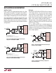
Full Rate CMOS Mode
In full rate CMOS mode the data outputs (D1_0 to D1_13
and D2_0 to D2_13), overflow (OF2, OF1), and the data
output clocks (CLKOUT
+
, CLKOUT
–
) have CMOS output
levels. The outputs are powered by OV
DD
and OGND which
are isolated from the A/D core power and ground. OV
DD
can range from 1.1V to 1.9V, allowing 1.2V through 1.8V
CMOS logic outputs.
For good performance the digital outputs should drive
minimal capacitive loads. If the load capacitance is larger
than 10pF a digital buffer should be used.
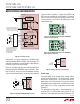
Double Data Rate CMOS Mode
In double data rate CMOS mode, two data bits are
multiplexed and output on each data pin. This reduces
the number of digital lines by fifteen, simplifying board
routing and reducing the number of input pins needed
to receive the data. The data outputs (D1_0_1, D1_2_3,
D1_4_5, D1_6_7, D1_8_9, D1_10_11, D1_12_13, D2_0_1,
D2_2_3, D2_4_5, D2_6_7, D2_8_9, D2_10_11,
D2_12_13), overflow (OF2_1), and the data output clocks
(CLKOUT
+
, CLKOUT
–
) have CMOS output levels. The out-
puts are powered by OV
DD
and OGND which are isolated
from the A/D core power and ground. OV
DD
can range
from 1.1V to 1.9V, allowing 1.2V through 1.8V CMOS logic
outputs. Note that the overflow for both ADC channels is
multiplexed onto the OF2_1 pin.
For good performance the digital outputs should drive
minimal capacitive loads. If the load capacitance is larger
than 10pF a digital buffer should be used.
When using double data rate CMOS at sample rates above
100Msps the SNR may degrade slightly, about 0.1dB to
0.3dB depending on load capacitance and board layout.
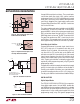
Double Data Rate LVDS Mode
In double data rate LVDS mode, two data bits are multi-
plexed and output on each differential output pair. There
are seven LVDS output pairs per ADC channel (D1_0_1
+
/
D1_0_1
–
through D1_12_13
+
/D1_12_13
–
and D2_0_1
+
/
D2_0_1
–
through D2_12_13
+
/D2_12_13
–
) for the digital
output data. Overflow (OF2_1
+
/OF2_1
–
) and the data
output clock (CLKOUT
+
/CLKOUT
–
) each have an LVDS
output pair. Note that the overflow for both ADC channels
is multiplexed onto the OF2_1
+
/OF2_1
–
output pair.
By default the outputs are standard LVDS levels: 3.5mA
output current and a 1.25V output common mode volt-
age. An external 100Ω differential termination resistor
is required for each LVDS output pair. The termination
resistors should be located as close as possible to the
LVDS receiver.
The outputs are powered by OV
DD
and OGND which are
isolated from the A/D core power and ground. In LVDS
mode, OV
DD
must be 1.8V.
Programmable LVDS Output Current
In LVDS mode, the default output driver current is 3.5mA.
This current can be adjusted by serially programming mode
control register A3. Available current levels are 1.75mA,
2.1mA, 2.5mA, 3mA, 3.5mA, 4mA and 4.5mA.
Optional LVDS Driver Internal Termination
In most cases using just an external 100Ω termination
resistor will give excellent LVDS signal integrity. In addi-
tion, an optional internal 100Ω termination resistor can
be enabled by serially programming mode control register
A3. The internal termination helps absorb any reflections
caused by imperfect termination at the receiver. When the
internal termination is enabled, the output driver current
is doubled to maintain the same output voltage swing.
Overflow Bit
The overflow output bit outputs a logic high when the analog
input is either overranged or underranged. The overflow
bit has the same pipeline latency as the data bits. In full
rate CMOS mode each ADC channel has its own overflow
pin (OF1 for channel 1, OF2 for channel 2). In DDR CMOS
or DDR LVDS mode the overflow for both ADC channels
is multiplexed onto the OF2_1 output.