LTC2172-14/ LTC2171-14/LTC2170-14 14-Bit, 65Msps/40Msps/ 25Msps Low Power Quad ADCs Description Features n n n n n n n n n n n n 4-Channel Simultaneous Sampling ADC 73.7dB SNR 90dB SFDR Low Power: 311mW/202mW/162mW Total, 78mW/51mW/41mW per Channel Single 1.
LTC2172-14/ LTC2171-14/LTC2170-14 Absolute Maximum Ratings Pin Configuration (Notes 1 and 2) OUT1B– OUT1B+ OUT1A– OUT1A+ GND SDO PAR/SER VREF GND SENSE VDD TOP VIEW VDD Supply Voltages VDD , OVDD............................................... –0.3V to 2V Analog Input Voltage (AIN +, AIN –, PAR/SER, SENSE) (Note 3)........... –0.3V to (VDD + 0.2V) Digital Input Voltage (ENC+, ENC–, CS, SDI, SCK) (Note 4)..................................... –0.3V to 3.9V SDO (Note 4)...........................
LTC2172-14/ LTC2171-14/LTC2170-14 Converter Characteristics The l denotes the specifications which apply over the full operating temperature range, otherwise specifications are at TA = 25°C. (Note 5) LTC2172-14 PARAMETER CONDITIONS Resolution (No Missing Codes) MIN l LTC2171-14 TYP MAX MIN ±1 3.25 14 LTC2170-14 TYP MAX MIN –2.75 ±1 2.75 14 TYP MAX UNITS –2.75 ±1 2.75 LSB LSB 14 Bits Integral Linearity Error Differential Analog Input (Note 6) l –3.
LTC2172-14/ LTC2171-14/LTC2170-14 Dynamic Accuracy The l denotes the specifications which apply over the full operating temperature range, otherwise specifications are at TA = 25°C. AIN = –1dBFS.
LTC2172-14/ LTC2171-14/LTC2170-14 Digital Inputs And Outputs The l denotes the specifications which apply over the full operating temperature range, otherwise specifications are at TA = 25°C. (Note 5) SYMBOL PARAMETER CONDITIONS MIN TYP MAX UNITS ENCODE INPUTS (ENC+, ENC– ) Differential Encode Mode (ENC– Not Tied to GND) VID Differential Input Voltage (Note 8) VICM Common Mode Input Voltage Internally Set Externally Set (Note 8) l 1.1 l 0.
LTC2172-14/ LTC2171-14/LTC2170-14 Power Requirements The l denotes the specifications which apply over the full operating temperature range, otherwise specifications are at TA = 25°C. (Note 9) LTC2172-14 SYMBOL PARAMETER CONDITIONS LTC2171-14 LTC2170-14 MIN TYP MAX MIN TYP MAX MIN TYP MAX UNITS VDD Analog Supply Voltage (Note 10) l 1.7 1.8 1.9 1.7 1.8 1.9 1.7 1.8 1.9 V OVDD Output Supply Voltage (Note 10) l 1.7 1.8 1.9 1.7 1.8 1.9 1.7 1.8 1.
LTC2172-14/ LTC2171-14/LTC2170-14 timing characteristics The l denotes the specifications which apply over the full operating temperature range, otherwise specifications are at TA = 25°C.
LTC2172-14/ LTC2171-14/LTC2170-14 Timing Diagrams 2-Lane Output Mode, 16-Bit Serialization* tAP ANALOG INPUT N+1 N tENCH tENCL ENC– ENC+ tSER DCO– DCO+ tDATA tFRAME FR– FR+ tSER tPD tSER OUT#A– OUT#A+ OUT#B– OUT#B+ D5 D3 D1 0 D13 D11 D9 D7 D5 D3 D1 0 D13 D11 D4 D2 D0 0 D12 D10 D8 D6 D4 D2 D0 0 D12 D10 SAMPLE N-6 D8 217214 TD01 SAMPLE N-4 SAMPLE N-5 D9 *SEE THE DIGITAL OUTPUTS SECTION 2-Lane Output Mode, 14-Bit Serialization tAP ANALOG INPUT N+2 N+1 N tENCH
LTC2172-14/ LTC2171-14/LTC2170-14 timing DIAGRAMS 2-Lane Output Mode, 12-Bit Serialization tAP ANALOG INPUT N+1 N tENCH tENCL ENC– ENC+ tSER DCO– DCO+ tDATA tFRAME FR+ FR– tPD tSER OUT#A– OUT#A+ OUT#B– OUT#B+ tSER D9 D7 D5 D3 D13 D11 D9 D7 D5 D3 D13 D11 D9 D8 D6 D4 D2 D12 D10 D8 D6 D4 D2 D12 D10 D8 SAMPLE N-6 SAMPLE N-5 217214 TD03 SAMPLE N-4 1-Lane Output Mode, 16-Bit Serialization tAP ANALOG INPUT N+1 N tENCH tENCL ENC– ENC+ tSER DCO– DCO+ tFRAME FR– FR
LTC2172-14/ LTC2171-14/LTC2170-14 timing DIAGRAMS 1-Lane Output Mode, 14-Bit Serialization tAP ANALOG INPUT N+1 N tENCH tENCL ENC– ENC+ tSER DCO– DCO+ tFRAME FR– FR+ OUT#A– OUT#A+ tDATA tSER tPD D3 D2 tSER D1 D0 SAMPLE N-6 D13 D12 D11 D10 D9 D8 D7 D6 D5 D4 D3 D2 D1 D0 SAMPLE N-5 D13 D12 D11 D10 217214 TD05 SAMPLE N-4 OUT#B+, OUT#B– ARE DISABLED 1-Lane Output Mode, 12-Bit Serialization tAP ANALOG INPUT N+1 N tENCH tENCL ENC– ENC+ tSER DCO– DCO+ tFRAME FR– FR+ O
LTC2172-14/ LTC2171-14/LTC2170-14 timing DIAGRAMS SPI Port Timing (Readback Mode) tDS tS tDH tSCK tH CS SCK tDO SDI SDO R/W A6 A5 A4 A3 A2 A1 A0 XX D7 HIGH IMPEDANCE XX D6 XX D5 XX D4 XX D3 XX D2 XX XX D1 D0 SPI Port Timing (Write Mode) CS SCK SDI SDO R/W HIGH IMPEDANCE A6 A5 A4 A3 A2 A1 A0 D7 D6 D5 D4 D3 D2 D1 D0 217214 TD07 21721014fb 11
LTC2172-14/ LTC2171-14/LTC2170-14 Typical Performance Characteristics LTC2172-14: Integral Nonlinearity (INL) LTC2172-14: Differential Nonlinearity (DNL) 2.0 1.5 0.8 –20 0.5 0 –0.5 –1.0 –30 0.4 AMPLITUDE (dBFS) DNL ERROR (LSB) INL ERROR (LSB) 0 –10 0.6 1.0 0.2 0 –0.2 –0.4 –0.8 0 4096 8192 12288 OUTPUT CODE –1.
LTC2172-14/ LTC2171-14/LTC2170-14 Typical Performance Characteristics LTC2172-14: SFDR vs Input Frequency, –1dBFS, 2V Range, 65Msps 95 80 110 100 SFDR (dBc AND dBFS) 90 85 80 75 80 70 60 dBc 50 60 40 30 40 30 20 10 10 0 50 100 150 200 250 300 INPUT FREQUENCY (MHz) 0 –80 –70 –60 –50 –40 –30 –20 –10 INPUT LEVEL (dBFS) 350 217214 G10 160 50 150 73 IOVDD (mA) 1-LANE, 3.5mA 30 2-LANE, 1.75mA 20 125 72 71 70 1-LANE, 1.
LTC2172-14/ LTC2171-14/LTC2170-14 Typical Performance Characteristics LTC2171-14: 8k Point FFT, fIN = 29MHz, –1dBFS, 40Msps 0 –10 –10 –20 –20 –20 –30 –30 –30 –40 –50 –60 –70 –80 AMPLITUDE (dBFS) 0 –10 AMPLITUDE (dBFS) AMPLITUDE (dBFS) 0 LTC2171-14: 8k Point FFT, fIN = 69MHz, –1dBFS, 40Msps –40 –50 –60 –70 –80 –40 –50 –60 –70 –80 –90 –100 –90 –100 –90 –100 –110 –120 –110 –120 –110 –120 0 20 10 FREQUENCY (MHz) 0 20 10 FREQUENCY (MHz) 217214 G18 217214 G20 LTC2171-14: Shorted
LTC2172-14/ LTC2171-14/LTC2170-14 Typical Performance Characteristics LTC2170-14: Integral Nonlinearity (INL) LTC2171-14: SNR vs SENSE, fIN = 5MHz, –1dBFS 1.5 72 1.0 INL ERROR (LSB) 73 SNR (dBFS) 71 70 69 –0.5 67 –1.5 66 –2.0 0.8 0.9 1 1.1 SENSE PIN (V) 1.2 1.3 0.6 0 –1.0 0.7 0.8 0.5 68 0.6 1.0 2.0 DNL ERROR (LSB) 74 0.2 0 –0.2 –0.4 –0.8 0 4096 8192 12288 OUTPUT CODE –1.
LTC2172-14/ LTC2171-14/LTC2170-14 Typical Performance Characteristics LTC2170-14: SFDR vs Input Frequency, –1dBFS, 2V Range, 25Msps LTC2170-14: SNR vs Input Frequency, –1dBFS, 2V Range, 25Msps 110 95 74 100 73 90 70 69 SFDR (dBc AND dBFS) SFDR (dBFS) SNR (dBFS) 71 85 80 75 68 0 100 150 200 250 300 INPUT FREQUENCY (MHz) 50 350 dBc 60 50 40 30 0 50 100 150 200 250 300 INPUT FREQUENCY (MHz) DCO Cycle-Cycle Jitter vs Serial Data Rate 74 350 73 300 PEAK-TO-PEAK JITTER (ps) 75 SNR (dB
LTC2172-14/ LTC2171-14/LTC2170-14 Pin Functions AIN1+ (Pin 1): Channel 1 Positive Differential Analog Input. AIN1– (Pin 2): Channel 1 Negative Differential Analog Input. VCM12 (Pin 3): Common Mode Bias Output, Nominally Equal to VDD /2. VCM should be used to bias the common mode of the analog inputs of channels 1 and 2. Bypass to ground with a 0.1µF ceramic capacitor. AIN2+ (Pin 4): Channel 2 Positive Differential Analog Input. AIN2– (Pin 5): Channel 2 Negative Differential Analog Input.
LTC2172-14/ LTC2171-14/LTC2170-14 Pin Functions PAR/SER (Pin 47): Programming Mode Selection Pin. Connect to ground to enable serial programming mode. CS, SCK, SDI and SDO become a serial interface that controls the A/D operating modes. Connect to VDD to enable parallel programming mode where CS, SCK, SDI and SDO become parallel logic inputs that control a reduced set of the A/D operating modes. PAR/SER should be connected directly to ground or the VDD of the part and not be driven by a logic signal.
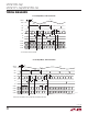
LTC2172-14/ LTC2171-14/LTC2170-14 Functional Block Diagram ENC+ ENC– 1.8V 1.8V VDD CHANNEL 1 ANALOG INPUT SAMPLEAND-HOLD 14-BIT ADC CORE CHANNEL 2 ANALOG INPUT SAMPLEAND-HOLD 14-BIT ADC CORE OVDD OUT1A PLL OUT1B OUT2A OUT2B DATA SERIALIZER CHANNEL 3 ANALOG INPUT OUT3A 14-BIT ADC CORE SAMPLEAND-HOLD OUT3B OUT4A CHANNEL 4 ANALOG INPUT VREF 1µF SAMPLEAND-HOLD 14-BIT ADC CORE OUT4B DATA CLOCKOUT 1.
LTC2172-14/ LTC2171-14/LTC2170-14 Applications Information CONVERTER OPERATION The LTC2172-14/LTC2171-14/LTC2170-14 are low power, 4-channel, 14-bit, 65Msps/40Msps/25Msps A/D converters that are powered by a single 1.8V supply. The analog inputs should be driven differentially. The encode input can be driven differentially for optimal jitter performance, or single-ended for lower power consumption. The digital outputs are serial LVDS to minimize the number of data lines.
LTC2172-14/ LTC2171-14/LTC2170-14 Applications Information Transformer Coupled Circuits Amplifier Circuits Figure 3 shows the analog input being driven by an RF transformer with a center-tapped secondary. The center tap is biased with VCM, setting the A/D input at its optimal DC level. At higher input frequencies a transmission line balun transformer (Figures 4 to 6) has better balance, resulting in lower A/D distortion. Figure 7 shows the analog input being driven by a high speed differential amplifier.
LTC2172-14/ LTC2171-14/LTC2170-14 Applications Information Reference Encode Input The LTC2172-14/LTC2171-14/LTC2170-14 has an internal 1.25V voltage reference. For a 2V input range using the internal reference, connect SENSE to VDD. For a 1V input range using the internal reference, connect SENSE to ground. For a 2V input range with an external reference, apply a 1.25V reference voltage to SENSE (Figure 9). The signal quality of the encode inputs strongly affects the A/D noise performance.
LTC2172-14/ LTC2171-14/LTC2170-14 Applications Information The differential encode mode is recommended for sinusoidal, PECL, or LVDS encode inputs (Figures 12 and 13). The encode inputs are internally biased to 1.2V through 10k equivalent resistance. The encode inputs can be taken above VDD (up to 3.6V), and the common mode range is from 1.1V to 1.6V. In the differential encode mode, ENC – should stay at least 200mV above ground to avoid falsely triggering the single-ended encode mode.
LTC2172-14/ LTC2171-14/LTC2170-14 Applications Information Table 1. Maximum Sampling Frequency for All Serialization Modes. Note That These Limits Are for the LTC2172-14. The Sampling Frequency for the Slower Speed Grades Cannot Exceed 40MHz (LTC2171-14) or 25MHz (LTC2170-14). SERIALIZATION MODE MAXIMUM SAMPLING FREQUENCY, fS (MHz) DCO FREQUENCY FR FREQUENCY SERIAL DATA RATE 2-Lane 16-Bit Serialization 65 4 • fS fS 8 • fS 2-Lane 14-Bit Serialization 65 3.5 • fS 0.
LTC2172-14/ LTC2171-14/LTC2170-14 Applications Information applied—an exclusive-OR operation is applied between the LSB and all other bits. The FR and DCO outputs are not affected. The output randomizer is enabled by serially programming mode control register A1. Digital Output Test Pattern To allow in-circuit testing of the digital interface to the A/D, there is a test mode that forces the A/D data outputs (D13-D0) of all channels to known values.
LTC2172-14/ LTC2171-14/LTC2170-14 Applications Information The first bit of the 16-bit input word is the R/W bit. The next seven bits are the address of the register (A6:A0). The final eight bits are the register data (D7:D0). If the R/W bit is low, the serial data (D7:D0) will be written to the register set by the address bits (A6:A0). If the R/W bit is high, data in the register set by the address bits (A6:A0) will be read back on the SDO pin (see the Timing Diagrams section).
LTC2172-14/ LTC2171-14/LTC2170-14 Applications Information REGISTER A2: OUTPUT MODE REGISTER (ADDRESS 02h) D7 ILVDS2 D6 D5 D4 D3 D2 D1 D0 ILVDS1 ILVDS0 TERMON OUTOFF OUTMODE2 OUTMODE1 OUTMODE0 Bits 7-5 ILVDS2:ILVDS0 LVDS Output Current Bits 000 = 3.5mA LVDS Output Driver Current 001 = 4.0mA LVDS Output Driver Current 010 = 4.5mA LVDS Output Driver Current 011 = Not Used 100 = 3.0mA LVDS Output Driver Current 101 = 2.5mA LVDS Output Driver Current 110 = 2.
LTC2172-14/ LTC2171-14/LTC2170-14 Applications Information GROUNDING AND BYPASSING The LTC2172-14/LTC2171-14/LTC2170-14 requires a printed circuit board with a clean unbroken ground plane. A multilayer board with an internal ground plane in the first layer beneath the ADC is recommended. Layout for the printed circuit board should ensure that digital and analog signal lines are separated as much as possible.
LTC2172-14/ LTC2171-14/LTC2170-14 Typical Applications Silkscreen Top Top Side Inner Layer 2 GND Inner Layer 3 21721014fb 29
LTC2172-14/ LTC2171-14/LTC2170-14 TYPICAL Applications Inner Layer 4 Inner Layer 5 Power Bottom Side Silkscreen Bottom 21721014fb 30
LTC2172-14/ LTC2171-14/LTC2170-14 TYPICAL Applications LTC2172 Schematic SENSE C17 1µF PAR/SER C4 1µF R14 1k SDO VDD C5 1µF C3 0.1µF 10 11 AIN3 12 AIN3 13 C59 0.1µF 14 OUT1B– OUT1B+ OUT1A– OUT1A+ SDO GND PAR/SER GND VREF 37 AIN2– DCO+ REFH DCO– LTC2172 OVDD REFH 35 34 33 REFL OGND REFL FR+ 32 AIN3+ FR– 31 AIN3– OUT3A+ 30 VCM34 OUT3A– 29 AIN4+ OUT3B+ 28 AIN4– OUT3B– 27 VDD AIN4 AIN4 DIGITAL OUTPUTS 36 C16 0.
LTC2172-14/ LTC2171-14/LTC2170-14 Package Description UKG Package 52-Lead Plastic QFN (7mm × 8mm) (Reference LTC DWG # 05-08-1729 Rev Ø) 7.50 ±0.05 6.10 ±0.05 5.50 REF (2 SIDES) 0.70 ±0.05 6.45 ±0.05 6.50 REF 7.10 ±0.05 8.50 ±0.05 (2 SIDES) 5.41 ±0.05 PACKAGE OUTLINE 0.25 ±0.05 0.50 BSC RECOMMENDED SOLDER PAD PITCH AND DIMENSIONS APPLY SOLDER MASK TO AREAS THAT ARE NOT SOLDERED 7.00 ± 0.10 (2 SIDES) 0.75 ± 0.05 0.00 – 0.05 R = 0.115 TYP 5.50 REF (2 SIDES) 51 52 0.40 ± 0.
LTC2172-14/ LTC2171-14/LTC2170-14 Revision History REV DATE DESCRIPTION A 03/10 Changed Sampling Frequency Max for LTC2171-14 from 45MHz to 40MHz in the Timing Characteristics section. 6 Added full part numbers to Grounding and Bypassing and Heat Transfer sections in Applications Information. 28 Revised Descriptions and Comments in the Related Parts section. 34 Corrected pin names for Pins 41-44 in the Pin Functions section.
LTC2172-14/ LTC2171-14/LTC2170-14 Related Parts PART NUMBER DESCRIPTION COMMENTS LTC2170-12/LTC217112/LTC2172-12 12-Bit, 25Msps/40Msps/65Msps 1.8V Quad ADCs, Ultralow Power 160mW/198mW/306mW, 71dB SNR, 90dB SFDR, Serial LVDS Outputs, 7mm × 8mm QFN-52 LTC2173-12/LTC217412/LTC2175-12 12-Bit, 80Msps/105Msps/125Msps 1.8V Quad ADCs, Ultralow Power 369mW/439mW/545mW, 70.6dB SNR, 88dB SFDR, Serial LVDS Outputs, 7mm × 8mm QFN-52 LTC2256-14/LTC225714/LTC2258-14 14-Bit, 25Msps/40Msps/65Msps 1.