
Datasheet


LTC2172-14/
LTC2171-14/LTC2170-14
7
21721014fb
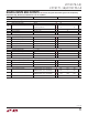
SYMBOL PARAMETER CONDITIONS MIN TYP MAX UNITS
Digital Data Outputs (R
TERM
= 100Ω Differential, C
L
= 2pF to GND on Each Output)
t
SER
Serial Data Bit Period 2-Lanes, 16-Bit Serialization
2-Lanes, 14-Bit Serialization
2-Lanes, 12-Bit Serialization
1-Lane, 16-Bit Serialization
1-Lane, 14-Bit Serialization
1-Lane, 12-Bit Serialization
1 / (8 • f
S
)
1 / (7 • f
S
)
1 / (6 • f
S
)
1 / (16 • f
S
)
1 / (14 • f
S
)
1 / (12 • f
S
)
s
s
s
s
s
s
t
FRAME
FR to DCO Delay (Note 8)
l
0.35 • t
SER
0.5 • t
SER
0.65 • t
SER
s
t
DATA
DATA to DCO Delay (Note 8)
l
0.35 • t
SER
0.5 • t
SER
0.65 • t
SER
s
t
PD
Propagation Delay (Note 8)
l
0.7n + 2 • t
SER
1.1n + 2 • t
SER
1.5n + 2 • t
SER
s
t
R
Output Rise Time Data, DCO, FR, 20% to 80% 0.17 ns
t
F
Output Fall Time Data, DCO, FR, 20% to 80% 0.17 ns
DCO Cycle-to-Cycle Jitter t
SER
= 1ns 60 ps
P-P
Pipeline Latency 6 Cycles
SPI Port Timing (Note 8)
t
SCK
SCK Period Write Mode
Readback Mode, C
SDO
= 20pF, R
PULLUP
= 2k
l
l
40
250
ns
ns
t
S
CS to SCK Set-Up Time
l
5 ns
t
H
SCK to CS Set-Up Time
l
5 ns
t
DS
SDI Set-Up Time
l
5 ns
t
DH
SDI Hold Time
l
5 ns
t
DO
SCK Falling to SDO Valid Readback Mode
C
SDO
= 20pF, R
PULLUP
= 2k
l
125 ns
Note 1: Stresses beyond those listed under Absolute Maximum Ratings
may cause permanent damage to the device. Exposure to any Absolute
Maximum Rating condition for extended periods may affect device
reliability and lifetime.
Note 2:
All voltage values are with respect to GND with GND and OGND
shorted (unless otherwise noted).
Note 3: When these pin voltages are taken below GND or above V
DD
, they
will be clamped by internal diodes. This product can handle input currents
of greater than 100mA below GND or above V
DD
without latchup.
Note 4: When these pin voltages are taken below GND they will be
clamped by internal diodes. When these pin voltages are taken above V
DD
they will not be clamped by internal diodes. This product can handle input
currents of greater than 100mA below GND without latchup.
Note 5: V
DD
= OV
DD
= 1.8V, f
SAMPLE
= 65MHz (LTC2172),
40MHz (LTC2171), or 25MHz (LTC2170), 2-lane output mode, differential
ENC
+
/ENC
–
= 2V
P-P
sine wave, input range = 2V
P-P
with differential drive,
unless otherwise noted.
Note 6: Integral nonlinearity is defined as the deviation of a code from a
best fit straight line to the transfer curve. The deviation is measured from
the center of the quantization band.
Note 7: Offset error is the offset voltage
measured from –0.5 LSB when
the output code flickers between 00 0000 0000 0000 and 11 1111 1111
1111 in 2’s complement output mode.
Note 8:
Guaranteed by design, not subject to test.
Note 9: V
DD
= OV
DD
= 1.8V, f
SAMPLE
= 65MHz (LTC2172), 40MHz
(LTC2171), or 25MHz (LTC2170), 2-lane output mode, ENC
+
= single-
ended 1.8V square wave, ENC
–
= 0V, input range = 2V
P-P
with differential
drive, unless otherwise noted. The supply current and power dissipation
specifications are totals for the entire chip, not per channel.
Note 10: Recommended operating conditions.
Note 11: The maximum sampling frequency depends on the speed grade
of the part and also which serialization mode is used. The maximum serial
data rate is 1000Mbps, so t
SER
must be greater than or equal to 1ns.
Note 12: Near-channel crosstalk refers to Ch. 1 to Ch.2, and Ch.3 to Ch.4.
Far-channel crosstalk refers to Ch.1 to Ch.3, Ch.1 to Ch.4, Ch.2 to Ch.3, and
Ch.2 to Ch.4.
TiMing characTerisTics
The l denotes the specifications which apply over the full operating temperature
range, otherwise specifications are at T
A
= 25°C. (Note 5)