LTC2175-12/ LTC2174-12/LTC2173-12 12-Bit, 125Msps/105Msps/ 80Msps Low Power Quad ADCs Features n n n n n n n n n n n n Description 4-Channel Simultaneous Sampling ADC 70.6dB SNR 88dB SFDR Low Power: 545mW/439mW/369mW Total, 136mW/110mW/92mW per Channel Single 1.
LTC2175-12/ LTC2174-12/LTC2173-12 Absolute Maximum Ratings Pin ConfigurationS (Notes 1, 2) OUT1B– OUT1B+ OUT1A– OUT1A+ GND SDO PAR/SER VREF GND SENSE VDD TOP VIEW VDD Supply Voltages VDD, OVDD................................................. –0.3V to 2V Analog Input Voltage (AIN+, AIN –, PAR/SER, SENSE) (Note 3)........... –0.3V to (VDD + 0.2V) Digital Input Voltage (ENC+, ENC–, CS, SDI, SCK) (Note 4)..................................... –0.3V to 3.9V SDO (Note 4)..............................
LTC2175-12/ LTC2174-12/LTC2173-12 Converter Characteristics The l denotes the specifications which apply over the full operating temperature range, otherwise specifications are at TA = 25°C. (Note 5) LTC2175-12 PARAMETER CONDITIONS MIN LTC2174-12 TYP MAX MIN LTC2173-12 TYP MAX MIN MAX UNITS l 12 Integral Linearity Error Differential Analog Input (Note 6) l –1 ±0.3 1 –1 ±0.3 1 –1 ±0.3 1 LSB Differential Linearity Error Differential Analog Input l –0.4 ±0.1 0.4 –0.4 ±0.1 0.
LTC2175-12/ LTC2174-12/LTC2173-12 Dynamic Accuracy The l denotes the specifications which apply over the full operating temperature range, otherwise specifications are at TA = 25°C. AIN = –1dBFS. (Note 5) LTC2175-12 SYMBOL PARAMETER CONDITIONS SNR Signal-to-Noise Ratio 5MHz Input 70MHz Input 140MHz Input SFDR S/(N+D) MAX LTC2174-12 MAX LTC2173-12 MIN TYP MIN TYP MIN TYP l 69.3 70.6 70.6 70.3 69.2 70.6 70.5 70.3 69.3 70.6 70.5 70.
LTC2175-12/ LTC2174-12/LTC2173-12 Digital Inputs and Outputs The l denotes the specifications which apply over the full operating temperature range, otherwise specifications are at TA = 25°C. (Note 5) SYMBOL PARAMETER CONDITIONS MIN TYP MAX UNITS ENCODE INPUTS (ENC+, ENC– ) Differential Encode Mode (ENC– Not Tied to GND) VID Differential Input Voltage (Note 8) l 0.2 VICM Common Mode Input Voltage Internally Set Externally Set (Note 8) l 1.1 l 0.
LTC2175-12/ LTC2174-12/LTC2173-12 Power Requirements The l denotes the specifications which apply over the full operating temperature range, otherwise specifications are at TA = 25°C. (Note 9) LTC2175-12 SYMBOL PARAMETER LTC2173-12 MIN TYP MAX MIN TYP MAX MIN TYP (Note 10) l 1.7 1.8 1.9 1.7 1.8 1.9 1.7 1.8 Output Supply Voltage (Note 10) l 1.7 1.8 1.9 1.7 1.8 1.9 1.7 1.8 1.
LTC2175-12/ LTC2174-12/LTC2173-12 timing characteristics The l denotes the specifications which apply over the full operating temperature range, otherwise specifications are at TA = 25°C.
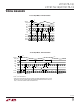
LTC2175-12/ LTC2174-12/LTC2173-12 Timing Diagrams 2-Lane Output Mode, 16-Bit Serialization tAP ANALOG INPUT N+1 N tENCH ENC– tENCL ENC+ tSER DCO– DCO+ tFRAME FR– FR+ tDATA tSER tPD OUT#A– OUT#A+ OUT#B– OUT#B+ tSER D3 D1 DX* 0 D11 D9 D7 D5 D3 D1 DX* 0 D11 D9 D7 D2 D0 DY* 0 D10 D8 D6 D4 D2 D0 DY* 0 D10 D8 D6 SAMPLE N-6 SAMPLE N-5 SAMPLE N-4 217512 TD01 *DX AND DY ARE EXTRA NON-DATA BITS FOR COMPLETE SOFTWARE COMPATIBILITY WITH THE 14-BIT VERSIONS OF THESE A/Ds.
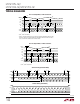
LTC2175-12/ LTC2174-12/LTC2173-12 timing DIAGRAMS 2-Lane Output Mode, 12-Bit Serialization tAP ANALOG INPUT N N+1 tENCH ENC– tENCL ENC+ tSER DCO– DCO+ tFRAME FR+ FR– OUT#A– OUT#A+ OUT#B– OUT#B+ tDATA tPD tSER tSER D7 D5 D3 D1 D11 D9 D7 D5 D3 D1 D11 D9 D7 D6 D4 D2 D0 D10 D8 D6 D4 D2 D0 D10 D8 D6 SAMPLE N-6 SAMPLE N-5 SAMPLE N-4 217512 TD03 1-Lane Output Mode, 16-Bit Serialization tAP ANALOG INPUT N+1 N tENCH ENC– tENCL ENC+ tSER DCO– DCO+ tFRAME FR– FR+ OUT#A– OU
LTC2175-12/ LTC2174-12/LTC2173-12 timing DIAGRAMS One-Lane Output Mode, 14-Bit Serialization tAP ANALOG INPUT N+1 N tENCH ENC– tENCL + ENC tSER DCO– + DCO tFRAME FR– FR+ OUT#A– OUT#A+ tDATA tSER tPD D1 D0 tSER DX* DY* D11 D10 D9 SAMPLE N-6 D8 D7 D6 D5 D4 D3 D2 D1 D0 DX* DY* D11 D10 D9 SAMPLE N-5 SAMPLE N-4 D8 217512 TD06 OUT#B+, OUT#B– ARE DISABLED *DX AND DY ARE EXTRA NON-DATA BITS FOR COMPLETE SOFTWARE COMPATIBILITY WITH THE 14-BIT VERSIONS OF THESE A/Ds.
LTC2175-12/ LTC2174-12/LTC2173-12 Typical Performance Characteristics LTC2175-12: Differential Nonlinearity (DNL) LTC2175-12: 8k Point FFT, fIN = 5MHz –1dBFS, 125Msps 1.0 1.0 0 0.8 0.8 –10 0.6 0.6 0.4 0.4 0.2 0 –0.2 –0.4 0 –0.2 –0.4 –0.6 –0.8 –0.8 –1.0 –1.0 1024 2048 3072 OUTPUT CODE 4096 –30 0.2 –0.
LTC2175-12/ LTC2174-12/LTC2173-12 Typical Performance Characteristics LTC2175-12: SFDR vs Input Frequency, –1dB, 2V Range, 125Msps 95 110 90 80 dBFS 100 80 75 80 70 dBc 60 60 SNR (dBc AND dBFS) 85 50 40 30 40 30 20 10 10 0 50 100 150 200 250 300 INPUT FREQUENCY (MHz) 0 –80 –70 –60 –50 –40 –30 –20 –10 INPUT LEVEL (dBFS) 350 217512 G10 2-LANE, 3.5mA 71 40 270 IOVDD (mA) 230 70 1-LANE, 3.5mA 30 2-LANE, 1.75mA 20 69 68 1-LANE, 1.
LTC2175-12/ LTC2174-12/LTC2173-12 Typical Performance Characteristics LTC2174-12: 8k Point FFT, fIN = 70MHz –1dBFS, 105Msps LTC2174-12: 8k Point FFT, fIN = 140MHz –1dBFS, 105Msps 0 0 –10 –10 –20 –20 –20 –30 –30 –30 –40 –50 –60 –70 –80 AMPLITUDE (dBFS) 0 –10 AMPLITUDE (dBFS) AMPLITUDE (dBFS) LTC2174-12: 8k Point FFT, fIN = 30MHz –1dBFS, 105Msps –40 –50 –60 –70 –80 –40 –50 –60 –70 –80 –90 –100 –90 –100 –90 –100 –110 –120 –110 –120 –110 –120 0 10 20 30 40 FREQUENCY (MHz) 50 0 10
LTC2175-12/ LTC2174-12/LTC2173-12 Typical Performance Characteristics LTC2174-12: SNR vs SENSE, fIN = 5MHz, –1dB LTC2173-12: Integral Nonlinearity (INL) 71 INL ERROR (LSB) SNR (dBFS) 70 69 68 67 66 0.6 0.7 0.8 0.9 1 1.1 SENSE PIN (V) 1.2 1.0 1.0 0.8 0.8 0.6 0.6 0.4 0.4 0.2 0 –0.2 –0.4 0 –0.2 –0.4 –0.6 –0.8 –0.8 0 1024 2048 3072 OUTPUT CODE –1.
LTC2175-12/ LTC2174-12/LTC2173-12 Typical Performance Characteristics LTC2173-12: SFDR vs Input Frequency, –1dB, 2V Range, 80Msps 95 71 90 70 85 69 LTC2173-12: SFDR vs Input Level, fIN = 70MHz, 2V Range, 80Msps 110 100 80 68 75 67 70 66 65 dBFS 90 SFDR (dBc AND dBFS) 72 SFDR (dBFS) SNR (dBFS) LTC2173-12: SNR vs Input Frequency, –1dB, 2V Range, 80Msps 80 70 dBc 60 50 40 30 20 10 0 50 100 150 200 250 300 INPUT FREQUENCY (MHz) 350 0 50 100 150 200 250 300 INPUT FREQUENCY (MHz) 217
LTC2175-12/ LTC2174-12/LTC2173-12 Pin Functions AIN1+ (Pin 1): Channel 1 Positive Differential Analog Input. AIN1– (Pin 2): Channel 1 Negative Differential Analog Input. VCM12 (Pin 3): Common Mode Bias Output, Nominally Equal to VDD/2. VCM should be used to bias the common mode of the analog inputs of channels 1 and 2. Bypass to ground with a 0.1µF ceramic capacitor. AIN2+ (Pin 4): Channel 2 Positive Differential Analog Input. AIN2– (Pin 5): Channel 2 Negative Differential Analog Input.
LTC2175-12/ LTC2174-12/LTC2173-12 Pin Functions VREF (Pin 48): Reference Voltage Output. Bypass to ground with a 1µF ceramic capacitor, nominally 1.25V. SENSE (Pin 50): Reference Programming Pin. Connecting SENSE to VDD selects the internal reference and a ±1V input range. Connecting SENSE to ground selects the internal reference and a ±0.5V input range. An external reference between 0.625V and 1.3V applied to SENSE selects an input range of ±0.8 • VSENSE.
LTC2175-12/ LTC2174-12/LTC2173-12 Functional Block Diagram 1.8V 1.
LTC2175-12/ LTC2174-12/LTC2173-12 Applications Information CONVERTER OPERATION The LTC2175-12/LTC2174-12/LTC2173-12 are low power, 4-channel, 12-bit, 125Msps/105Msps/80Msps A/D converters that are powered by a single 1.8V supply. The analog inputs should be driven differentially. The encode input can be driven differentially for optimal jitter performance, or single-ended for lower power consumption. The digital outputs are serial LVDS to minimize the number of data lines.
LTC2175-12/ LTC2174-12/LTC2173-12 Applications Information tap is biased with VCM, setting the A/D input at its optimal DC level. At higher input frequencies a transmission line balun transformer (Figures 4 to 6) has better balance, resulting in lower A/D distortion. Amplifier Circuits Figure 7 shows the analog input being driven by a high speed differential amplifier.
LTC2175-12/ LTC2174-12/LTC2173-12 Applications Information ground. For a 2V input range with an external reference, apply a 1.25V reference voltage to SENSE (Figure 9). and REFL should be as close to the pins as possible (not on the backside of the circuit board). The input range can be adjusted by applying a voltage to SENSE that is between 0.625V and 1.30V. The input range will then be 1.6 • VSENSE.
LTC2175-12/ LTC2174-12/LTC2173-12 Applications Information The differential encode mode is recommended for sinusoidal, PECL, or LVDS encode inputs (Figures 12 and 13). The encode inputs are internally biased to 1.2V through 10k equivalent resistance. The encode inputs can be taken above VDD (up to 3.6V), and the common mode range is from 1.1V to 1.6V. In the differential encode mode, ENC– should stay at least 200mV above ground to avoid falsely triggering the single-ended encode mode.
LTC2175-12/ LTC2174-12/LTC2173-12 Applications Information DIGITAL OUTPUTS The digital outputs of the LTC2175-12/LTC2174-12/ LTC2173-12 are serialized LVDS signals. Each channel outputs two bits at a time (2-lane mode). At lower sampling rates there is a one bit per channel option (1-lane mode). The data can be serialized with 16, 14, or 12-bit serialization (see timing diagrams for details). The output data should be latched on the rising and falling edges of the data clock out (DCO).
LTC2175-12/ LTC2174-12/LTC2173-12 Applications Information DATA FORMAT Table 2 shows the relationship between the analog input voltage and the digital data output bits. By default the output data format is offset binary. The 2’s complement format can be selected by serially programming mode control register A1. In addition to the 12 data bits (D11 - D0), two additional bits (DX and DY) are sent out in the 14-bit and 16-bit serialization modes.
LTC2175-12/ LTC2174-12/LTC2173-12 Applications Information In nap mode any combination of A/D channels can be powered down while the internal reference circuits and the PLL stay active, allowing faster wakeup than from sleep mode. Recovering from nap mode requires at least 100 clock cycles.
LTC2175-12/ LTC2174-12/LTC2173-12 Applications Information Software Reset If serial programming is used, the mode control registers should be programmed as soon as possible after the power supplies turn on and are stable. The first serial command must be a software reset which will reset all register data bits to logic 0. To perform a software reset, bit D7 in the reset register is written with a logic 1. After the reset SPI write command is complete, bit D7 is automatically set back to zero.
LTC2175-12/ LTC2174-12/LTC2173-12 Applications Information Bits 4-0 SLEEP: NAP_4:NAP_1 Sleep/Nap Mode Control Bits 00000 = Normal Operation 0XXX1 = Channel 1 in Nap Mode 0XX1X = Channel 2 in Nap Mode 0X1XX = Channel 3 in Nap Mode 01XXX = Channel 4 in Nap Mode 1XXXX = Sleep Mode. All Channels are Disabled Note: Any Combination of Channels Can Be Placed in Nap Mode.
LTC2175-12/ LTC2174-12/LTC2173-12 Typical Applications Silkscreen Top Top Side 21754312fa 28
LTC2175-12/ LTC2174-12/LTC2173-12 TYPICAL Applications Inner Layer 2 GND Inner Layer 3 Inner Layer 4 Inner Layer 5 Power 21754312fa 29
LTC2175-12/ LTC2174-12/LTC2173-12 TYPICAL Applications Bottom Side Silkscreen Bottom 21754312fa 30
LTC2175-12/ LTC2174-12/LTC2173-12 TYPICAL Applications LTC2175 Schematic SENSE R14 1k C17 1µF PAR/SER C4 1µF SDO VDD C5 1µF 10 11 R93 100 AIN3 12 AIN3 13 C59 0.1µF AIN4 14 R94 100 OUT1B– OUT1B+ OUT1A– OUT1A+ SDO GND PAR/SER GND VREF AIN2 REFH DCO– LTC2175 35 34 REFH OVDD REFL OGND REFL FR+ 32 AIN3+ FR– 31 AIN3– OUT3A+ 30 VCM34 OUT3A– 29 33 AIN4 + OUT3B+ 28 AIN4– OUT3B– 27 AIN4 DIGITAL OUTPUTS 36 C16 0.1µF OVDD DIGITAL OUTPUTS OUT4A+ 9 C3 0.
LTC2175-12/ LTC2174-12/LTC2173-12 Package Description UKG Package 52-Lead Plastic QFN (7mm × 8mm) (Reference LTC DWG # 05-08-1729 Rev Ø) 7.50 ±0.05 6.10 ±0.05 5.50 REF (2 SIDES) 0.70 ±0.05 6.45 ±0.05 6.50 REF 7.10 ±0.05 8.50 ±0.05 (2 SIDES) 5.41 ±0.05 PACKAGE OUTLINE 0.25 ±0.05 0.50 BSC RECOMMENDED SOLDER PAD PITCH AND DIMENSIONS APPLY SOLDER MASK TO AREAS THAT ARE NOT SOLDERED 7.00 ± 0.10 (2 SIDES) 0.75 ± 0.05 0.00 – 0.05 R = 0.115 TYP 5.50 REF (2 SIDES) 51 52 0.40 ± 0.
LTC2175-12/ LTC2174-12/LTC2173-12 Revision History REV DATE DESCRIPTION PAGE NUMBER A 6/11 Corrected part numbers in Description. 1 Revised Software Reset paragraph and Table 4 in Applications Information section. 26 Added VDD to LTC2175 Schematic in Typical Applications section. 31 21754312fa Information furnished by Linear Technology Corporation is believed to be accurate and reliable. However, no responsibility is assumed for its use.
LTC2175-12/ LTC2174-12/LTC2173-12 Related Parts PART NUMBER DESCRIPTION COMMENTS ADCs LTC2170-14/LTC2171-14/ 14-Bit, 25Msps/40Msps/65Msps LTC2172-14 1.8V Quad ADCs, Ultralow Power 178mW/234mW/360mW, 73.4dB SNR, 85dB SFDR, Serial LVDS Outputs, 7mm × 8mm QFN-52 LTC2170-12/LTC2171-12/ 12-Bit, 25Msps/40Msps/65Msps LTC2172-12 1.8V Quad ADCs, Ultralow Power 178mW/234mW/360mW, 70.5dB SNR, 85dB SFDR, Serial LVDS Outputs, 7mm × 8mm QFN-52 LTC2173-14/LTC2174-14/ 14-Bit, 80Msps/105Msps/125Msps LTC2175-14 1.