
Datasheet


LTC2175-12/
LTC2174-12/LTC2173-12
24
21754312fa
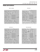
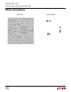
Table 2. Output Codes vs Input Voltage
A
IN
+
– A
IN
–
(2V RANGE)
D11-D0
(OFFSET BINARY)
D11-D0
(2’s COMPLEMENT)
D
X
, D
Y
>+1.000000V
+0.999512V
+0.999024V
1111 1111 1111
1111 1111 1111
1111 1111 1110
0111 1111 1111
0111 1111 1111
0111 1111 1110
11
00
00
+0.000488V
0.000000V
–0.000488V
–0.000976V
1000 0000 0001
1000 0000 0000
0111 1111 1111
0111 1111 1110
0000 0000 0001
0000 0000 0000
1111 1111 1111
1111 1111 1110
00
00
00
00
–0.999512V
–1.000000V
≤–1.000000V
0000 0000 0001
0000 0000 0000
0000 0000 0000
1000 0000 0001
1000 0000 0000
1000 0000 0000
00
00
00
applicaTions inForMaTion
DATA FORMAT
Table 2 shows the relationship between the analog input
voltage and the digital data output bits. By default the
output data format is offset binary. The 2’s complement
format can be selected by serially programming mode
control register A1.
In addition to the 12 data bits (D11 - D0), two additional
bits (D
X
and D
Y
) are sent out in the 14-bit and 16-bit
serialization modes. These extra bits are to ensure com-
plete software compatibility with the 14-bit versions of
these A/Ds. During normal operation when the analog
inputs are not overranged, D
X
and D
Y
are always logic 0.
When the analog inputs are overranged positive, D
X
and
D
Y
become logic 1. When the analog inputs are over-
ranged negative, D
X
and D
Y
become logic 0. D
X
and D
Y
can also be controlled by the digital output test pattern.
See the Timing Diagrams section for more information.
output before it is transmitted off chip, these unwanted
tones can be randomized which reduces the unwanted
tone amplitude.
The digital output is randomized by applying an exclusive-
OR logic operation between the LSB and all other data
output bits. To decode, the reverse operation is applied
—an exclusive-OR operation is applied between the LSB
and all other bits. The FR and DCO outputs are not affected.
The output randomizer is enabled by serially programming
mode control register A1.
Digital Output Test Pattern
To allow in-circuit testing of the digital interface to the
A/D, there is a test mode that forces the A/D data outputs
(D11-D0, D
X
, D
Y
) of all channels to known values. The
digital output test patterns are enabled by serially program-
ming mode control registers A3 and A4. When enabled,
the test patterns override all other formatting modes: 2’s
complement and randomizer.
Output Disable
The digital outputs may be disabled by serially programming
mode control register A2. The current drive for all digital
outputs including DCO and FR are disabled to save power
or enable in-circuit testing. When disabled the common
mode of each output pair becomes high impedance, but
the differential impedance may remain low.
Sleep and Nap Modes
The A/D may be placed in sleep or nap modes to conserve
power. In sleep mode the entire chip is powered down, re-
sulting in 1mW power consumption. Sleep mode is enabled
by mode control register A1 (serial programming mode),
or by SDI (parallel programming mode). The amount of
time required to recover from sleep mode depends on the
size of the bypass capacitors on V
REF
, REFH, and REFL.
For the suggested values in Figure 8, the A/D will stabilize
after 2ms.
Digital Output Randomizer
Interference from the A/D digital outputs is sometimes
unavoidable. Digital interference may be from capacitive or
inductive coupling or coupling through the ground plane.
Even a tiny coupling factor can cause unwanted tones
in the ADC output spectrum. By randomizing the digital