
Datasheet

LTC2255/LTC2254
16
22554fa
APPLICATIO S I FOR ATIO
WUUU
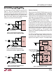
pins are needed to reduce package inductance. Bypass
capacitors must be connected as shown in Figure 9.
Other voltage ranges in-between the pin selectable ranges
can be programmed with two external resistors as shown
in Figure 10. An external reference can be used by applying
its output directly or through a resistor divider to SENSE.
It is not recommended to drive the SENSE pin with a logic
device. The SENSE pin should be tied to the appropriate
level as close to the converter as possible. If the SENSE pin
is driven externally, it should be bypassed to ground as
close to the device as possible with a 1µF ceramic capacitor.
Input Range
The input range can be set based on the application. The
2V input range will provide the best signal-to-noise perfor-
mance while maintaining excellent SFDR. The 1V input
range will have better SFDR performance, but the SNR will
degrade by 5.7dB.
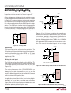
Driving the Clock Input
The CLK input can be driven directly with a CMOS or TTL
level signal. A sinusoidal clock can also be used along with
a low-jitter squaring circuit before the CLK pin (see
Figure 11).
The noise performance of the LTC2255/LTC2254 can
depend on the clock signal quality as much as on the
analog input. Any noise present on the clock signal will
result in additional aperture jitter that will be RMS summed
with the inherent ADC aperture jitter.
In applications where jitter is critical, such as when digitiz-
ing high input frequencies, use as large an amplitude as
possible. Also, if the ADC is clocked with a sinusoidal
signal, filter the CLK signal to reduce wideband noise and
distortion products generated by the source.
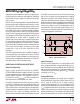
Figure 11. Sinusoidal Single-Ended CLK Drive
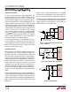
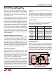
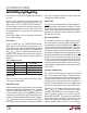
Figures 12 and 13 show alternatives for converting a
differential clock to the single-ended CLK input. The use of
a transformer provides no incremental contribution to
phase noise. The LVDS or PECL to CMOS translators
provide little degradation below 70MHz, but at 140MHz
will degrade the SNR compared to the transformer solu-
tion. The nature of the received signals also has a large
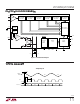
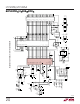
Figure 10. 1.5V Range ADC
V
CM
SENSE
1.5V
0.75V
2.2µF
12k
1µF
12k
22554 F10
LTC2255/
LTC2254
CLK
50Ω
0.1µF
0.1µF
4.7µF
1k
1k
FERRITE
BEAD
CLEAN
SUPPLY
SINUSOIDAL
CLOCK
INPUT
22554 F11
NC7SVU04
LTC2255/
LTC2254
CLK
100Ω
0.1µF
4.7µF
FERRITE
BEAD
CLEAN
SUPPLY
IF LVDS USE FIN1002 OR FIN1018.
FOR PECL, USE AZ1000ELT21 OR SIMILAR
22554 F12
LTC2255/
LTC2254
CLK
5pF-30pF
ETC1-1T
0.1µF
V
CM
FERRITE
BEAD
DIFFERENTIAL
CLOCK
INPUT
22554 F13
LTC2255/
LTC2254
Figure 13. LVDS or PECL CLK Drive Using a Transformer
Figure 12. CLK Drive Using an LVDS or PECL to CMOS Converter