
Datasheet

LTC2298/LTC2297/LTC2296
16
229876fa
sensitive applications, the analog inputs can be driven
single-ended with slightly worse harmonic distortion. The
CLK input is single-ended. The LTC2298/LTC2297/
LTC2296 have two phases of operation, determined by the
state of the CLK input pin.
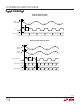
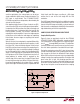
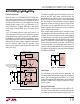
Each pipelined stage shown in Figure 1 contains an ADC,
a reconstruction DAC and an interstage residue amplifier.
In operation, the ADC quantizes the input to the stage and
the quantized value is subtracted from the input by the
DAC to produce a residue. The residue is amplified and
output by the residue amplifier. Successive stages operate
out of phase so that when the odd stages are outputting
their residue, the even stages are acquiring that residue
and vice versa.
When CLK is low, the analog input is sampled differentially
directly onto the input sample-and-hold capacitors, inside
the “Input S/H” shown in the block diagram. At the instant
that CLK transitions from low to high, the sampled input is
held. While CLK is high, the held input voltage is buffered
by the S/H amplifier which drives the first pipelined ADC
stage. The first stage acquires the output of the S/H during
this high phase of CLK. When CLK goes back low, the first
stage produces its residue which is acquired by the
second stage. At the same time, the input S/H goes back
to acquiring the analog input. When CLK goes back high,
the second stage produces its residue which is acquired
by the third stage. An identical process is repeated for the
APPLICATIO S I FOR ATIO
WUU
U
third, fourth and fifth stages, resulting in a fifth stage
residue that is sent to the sixth stage ADC for final
evaluation.
Each ADC stage following the first has additional range to
accommodate flash and amplifier offset errors. Results
from all of the ADC stages are digitally synchronized such
that the results can be properly combined in the correction
logic before being sent to the output buffer.
SAMPLE/HOLD OPERATION AND INPUT DRIVE
Sample/Hold Operation
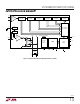
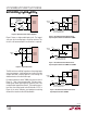
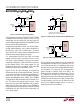
Figure 2 shows an equivalent circuit for the LTC2298/
LTC2297/LTC2296 CMOS differential sample-and-hold.
The analog inputs are connected to the sampling capaci-
tors (C
SAMPLE
) through NMOS transistors. The capacitors
shown attached to each input (C
PARASITIC
) are the summa-
tion of all other capacitance associated with each input.
During the sample phase when CLK is low, the transistors
connect the analog inputs to the sampling capacitors and
they charge to and track the differential input voltage.
When CLK transitions from low to high, the sampled input
voltage is held on the sampling capacitors. During the hold
phase when CLK is high, the sampling capacitors are
disconnected from the input and the held voltage is passed
to the ADC core for processing. As CLK transitions from
high to low, the inputs are reconnected to the sampling
Figure 2. Equivalent Input Circuit
V
DD
V
DD
V
DD
15Ω
15Ω
C
PARASITIC
1pF
C
PARASITIC
1pF
C
SAMPLE
4pF
C
SAMPLE
4pF
LTC2298/LTC2297/LTC2296
A
IN
+
A
IN
–
CLK
229876 F02