
Datasheet


LTC2351-14
1
235114fb
FEATURES
APPLICATIONS
DESCRIPTION
6-Channel, 14-Bit, 1.5Msps
Simultaneous Sampling ADC
with Shutdown
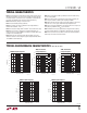
The LTC
®
2351-14 is a 14-bit, 1.5Msps ADC with six simul-
taneously sampled differential inputs. The device draws
only 5.5mA from a single 3V supply, and comes in a tiny
32-pin (5mm × 5mm) QFN package. A sleep shutdown
mode further reduces power consumption to 12μW. The
combination of low power and tiny package makes the
LTC2351-14 suitable for portable applications.
The LTC2351-14 contains six separate differential inputs
that are sampled simultaneously on the rising edge of the
CONV signal. These six sampled inputs are then converted
at a rate of 250ksps per channel.
The 83dB common mode rejection allows users to eliminate
ground loops and common mode noise by measuring
signals differentially from the source.
The device converts 0V to 2.5V unipolar inputs differentially,
or ±1.25V bipolar inputs also differentially, depending on the
state of the BIP pin. Any analog input may swing rail-to-rail
as long as the differential input range is maintained.
The conversion sequence can be abbreviated to convert
fewer than six channels, depending on the logic state of
the SEL2, SEL1 and SEL0 inputs.
The serial interface sends out the six conversion results in 96
clocks for compatibility with standard serial interfaces.
n
1.5Msps ADC with Six Simultaneously Sampled
Differential Inputs
n
250ksps Throughput per Channel
n
75dB SINAD
n
Low Power Dissipation: 16.5mW
n
3V Single Supply Operation
n
2.5V Internal Bandgap Reference, Can Be Overdriven
with External Reference
n
3-Wire SPI-Compatible Serial Interface
n
Internal Conversion Triggered by CONV
n
Sleep (12μW) Shutdown Mode
n
NAP (4.5mW) Shutdown Mode
n
0V to 2.5V Unipolar, or ±1.25V Bipolar Differential
Input Range
n
83dB Common Mode Rejection
n
Tiny 32-Pin (5mm × 5mm) QFN Package
n
Multiphase Power Measurement
n
Multiphase Motor Control
n
Data Acquisition Systems
n
Uninterruptable Power Supplies
L, LT, LTC and LTM are registered trademarks of Linear Technology Corporation.
All other trademarks are the property of their respective owners. Protected by U.S. Patents,
including 6084440, 6522187.
BLOCK DIAGRAM
–
+
4
5
25
24
–
+
7 6912
13
1619 8
CH0
–
CH0
+
CH1
–
CH1
+
10
11
–
+
1415
CH2
–
CH2
+
CH3
–
CH3
+
–
+
17
18
–
+
2021
S AND H S AND H S AND H S AND H S AND H
CH4
–
CH4
+
CH5
–
CH5
+
MUX
V
REF
10μF
BIP SEL2 SEL1 SEL0GND
2.5V
REFERENCE
1.5Msps
14-BIT ADC
14-BIT LATCH 5
14-BIT LATCH 4
14-BIT LATCH 3
14-BIT LATCH 2
14-BIT LATCH 1
14-BIT LATCH 0
10μF 3V
V
CC
V
DD
2629232233 27 28
2
1
SD0
0.1μF
3
OV
DD
3V
32
SCK
31
DGND
OGND
30
CONV
THREE-
STATE
SERIAL
OUTPUT
PORT
TIMING
LOGIC
235114 TA01
–
+
S AND H