
Datasheet


LTC2351-14
4
235114fb
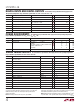
POWER REQUIREMENTS
The l denotes the specifi cations which apply over the full operating temperature
range, otherwise specifi cations are at T
A
= 25°C. V
DD
= V
CC
= 3V.
TIMING CHARACTERISTICS
Note 1: Stresses beyond those listed under Absolute Maximum Ratings
may cause permanent damage to the device. Exposure to any Absolute
Maximum Rating condition for extended periods may affect device
reliabilty and lifetime.
Note 2: All voltage values are with respect to ground GND.
The l denotes the specifi cations which apply over the full operating temperature
range, otherwise specifi cations are at T
A
= 25°C. V
DD
= 3V.
SYMBOL PARAMETER CONDITIONS MIN TYP MAX UNITS
V
DD
, V
CC
Supply Voltage 2.7 3 3.6 V
I
DD
+ I
CC
Supply Current Active Mode, f
SAMPLE
= 1.5Msps
Nap Mode
Active Mode, f
SAMPLE
= 1.5Msps (LTC2351H-14)
Nap Mode (LTC2351H-14)
Sleep Mode
l
l
l
l
5.5
1.5
6
1.8
4
8
2
9
2.5
15
mA
mA
mA
mA
μA
P
D
Power Dissipation Active Mode with SCK, f
SAMPLE
= 1.5Msps 16.5 mW
SYMBOL PARAMETER CONDITIONS MIN TYP MAX UNITS
f
SAMPLE(MAX)
Maximum Sampling Rate per Channel
(Conversion Rate)
l
250 kHz
t
THROUGHPUT
Minimum Sampling Period (Conversion + Acquisiton Period)
l
4μs
t
SCK
Clock Period (Note 16)
l
40 10000 ns
t
CONV
Conversion Time (Notes 6, 17) 96 SCLK cycles
t
1
Minimum High or Low SCLK Pulse Width (Note 6) 2 ns
t
2
CONV to SCK Setup Time (Notes 6, 10) 3 10000 ns
t
3
SCK Before CONV (Note 6) 0 ns
t
4
Minimum High or Low CONV Pulse Width (Note 6) 4 ns
t
5
SCK↑ to Sample Mode
(Note 6) 4 ns
t
6
CONV↑ to Hold Mode
(Notes 6, 11) 1.2 ns
t
7
96th SCK↑ to CONV↑ Interval (Affects Acquisition Period)
(Notes 6, 7, 13) 45 ns
t
8
Minimum Delay from SCK to Valid Bits 0 Through 11 (Notes 6, 12) 8 ns
t
9
SCK↑ to Hi-Z at SDO
(Notes 6, 12) 6 ns
t
10
Previous SDO Bit Remains Valid After SCK (Notes 6, 12) 2 ns
t
11
V
REF
Settling Time After Sleep-to-Wake Transition (Notes 6, 14) 2 ms
Note 3: When these pins are taken below GND or above V
DD
, they will be
clamped by internal diodes. This product can handle input currents greater
than 100mA below GND or greater than V
DD
without latchup.
Note 4: Offset and range specifi cations apply for a single-ended CH0
+
– CH5
+
input with CH0
–
– CH5
–
grounded and using the internal 2.5V reference.
I
IN
Digital Input Current V
IN
= 0V to V
DD
l
±10 μA
C
IN
Digital Input Capacitance 5pF
V
OH
High Level Output Voltage V
DD
= 3V, I
OUT
= –200μA
l
2.5 2.9 V
V
OL
Low Level Output Voltage V
DD
= 2.7V, I
OUT
= 160μA
V
DD
= 2.7V, I
OUT
= 1.6mA
l
0.05
0.4
V
V
I
OZ
Hi-Z Output Leakage D
OUT
V
OUT
= 0V and V
DD
l
±10 μA
C
OZ
Hi-Z Output Capacitance D
OUT
1pF
I
SOURCE
Output Short-Circuit Source Current V
OUT
= 0V, V
DD
= 3V 20 mA
I
SINK
Output Short-Circuit Sink Current V
OUT
= V
DD
= 3V 15 mA
DIGITAL INPUTS AND DIGITAL OUTPUTS
The l denotes the specifi cations which apply over the
full operating temperature range, otherwise specifi cations are at T
A
= 25°C. V
DD
= V
CC
= 3V.