
Datasheet


LTC2351-14
5
235114fb
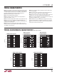
TYPICAL PERFORMANCE CHARACTERISTICS
SINAD vs Input Frequency
THD, 2nd and 3rd
vs Input Frequency
THD, 2nd and 3rd
vs Input Frequency
SFDR vs Input Frequency SNR vs Input Frequency
V
DD
= 3V, T
A
= 25°C
FREQUENCY (MHz)
56
65
62
59
77
74
71
68
235114 G01
SINAD (dB)
0.1
10
1
FREQUENCY (MHz)
0.1
–110
THD, 2nd, 3rd (dB)
–98
–86
–74
–62
110
235114 G02
–50
–104
–92
–80
–68
–56
UNIPOLAR SINGLE-ENDED
THD
3rd
2nd
FREQUENCY (MHz)
0.1
–110
THD, 2nd, 3rd (dB)
–98
–86
–74
–62
110
235114 G03
–50
–104
–92
–80
–68
–56
BIPOLAR SINGLE-ENDED
THD
2nd
3rd
FREQUENCY (MHz)
50
68
62
56
92
86
80
74
235114 G04
SFDR (dB)
0.1
10
1
FREQUENCY (MHz)
0.1
SNR (dB)
56
62
59
65
68
71
74
110
235114 G05
77
Note 5: Integral linearity is tested with an external 2.55V reference and is
defi ned as the deviation of a code from the straight line passing through
the actual endpoints of a transfer curve. The deviation is measured from
the center of quantization band. Linearity is tested for CH0 only.
Note 6: Guaranteed by design, not subject to test.
Note 7: Recommended operating conditions.
Note 8: The analog input range is defi ned for the voltage difference
between CHx
+
and CHx
–
, x = 0–5.
Note 9: The absolute voltage at CHx
+
and CHx
–
must be within this range.
Note 10: If less than 3ns is allowed, the output data will appear one
clock cycle later. It is best for CONV to rise half a clock before SCK, when
running the clock at rated speed.
Note 11: Not the same as aperture delay. Aperture delay (1ns) is the
difference between the 2.2ns delay through the sample-and-hold and the
1.2ns CONV to Hold mode delay.
Note 12: The rising edge of SCK is guaranteed to catch the data coming
out into a storage latch.
Note 13: The time period for acquiring the input signal is started by the
96th rising clock and it is ended by the rising edge of CONV.
Note 14: The internal reference settles in 2ms after it wakes up from sleep
mode with one or more cycles at SCK and a 10μF capacitive load.
Note 15: The full power bandwidth is the frequency where the output code
swing drops by 3dB with a 2.5V
P-P
input sine wave.
Note 16: Maximum clock period guarantees analog performance during
conversion. Output data can be read with an arbitrarily long clock period.
Note 17: The conversion process takes 16 clocks for each channel that is
enabled, up to 96 clocks for all six channels.
TIMING CHARACTERISTICS