
Datasheet


LTC2351-14
7
235114fb
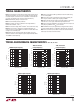
PIN FUNCTIONS
SDO (Pin 1): Three-State Serial Data Output. Each set
of six output data words represent the six analog input
channels at the start of the previous conversion. Data for
CH0 comes out fi rst and data for CH5 comes out last. Each
data word comes out MSB fi rst.
OGND (Pin 2): Ground Return for SDO Currents. Connect
to the solid ground plane.
OV
DD
(Pin 3): Power Supply for the SDO Pin. OV
DD
must be no more than 300mV higher than V
DD
and can
be brought to a lower voltage to interface to low voltage
logic families. The unloaded HIGH state at SDO is at the
potential of OV
DD
.
CH0
+
(Pin 4): Noninverting Channel 0. CH0
+
operates
fully differentially with respect to CH0
–
with a 0V to 2.5V,
or ±1.25V differential swing and a 0V to V
DD
absolute
input range.
CH0
–
(Pin 5): Inverting Channel 0. CH0
–
operates fully
differentially with respect to CH0
+
with a –2.5V to 0V,
or ±1.25V differential swing and a 0V to V
DD
absolute
input range.
GND (Pins 6, 9, 12, 13, 16, 19): Analog Grounds. These
ground pins must be tied directly to the solid ground plane
under the part. Analog signal currents fl ow through these
connections.
CH1
+
(Pin 7): Noninverting Channel 1. CH1
+
operates
fully differentially with respect to CH1
–
with a 0V to 2.5V,
or ±1.25V differential swing and a 0V to V
DD
absolute
input range.
CH1
–
(Pin 8): Inverting Channel 1. CH1
–
operates fully
differentially with respect to CH1
+
with a –2.5V to 0V,
or ±1.25V differential swing and a 0V to V
DD
absolute
input range.
CH2
+
(Pin 10): Noninverting Channel 2. CH2
+
operates
fully differentially with respect to CH2
–
with a 0V to 2.5V,
or ±1.25V differential swing and a 0V to V
DD
absolute
input range.
CH2
–
(Pin 11): Inverting Channel 2. CH2
–
operates fully
differentially with respect to CH2
+
with a –2.5V to 0V,
or ±1.25V differential swing and a 0V to V
DD
absolute
input range.
CH3
+
(Pin 14): Noninverting Channel 3. CH3
+
operates
fully differentially with respect to CH3
–
with a 0V to 2.5V,
or ±1.25V differential swing and a 0V to V
DD
absolute
input range.
CH3
–
(Pin 15): Inverting Channel 3. CH3
–
operates fully
differentially with respect to CH3
+
with a –2.5V to 0V,
or ±1.25V differential swing and a 0V to V
DD
absolute
input range.
CH4
+
(Pin 17): Noninverting Channel 4. CH4
+
operates
fully differentially with respect to CH4
–
with a 0V to 2.5V,
or ±1.25V differential swing and a 0V to V
DD
absolute
input range.
CH4
–
(Pin 18): Inverting Channel 4. CH4
–
operates fully
differentially with respect to CH4
+
with a –2.5V to 0V, or
±1.25V differential swing and a 0V to V
DD
absolute input
range.
CH5
+
(Pin 20): Noninverting Channel 5. CH5
+
operates
fully differentially with respect to CH5
–
with a 0V to 2.5V,
or ±1.25V differential swing and a 0V to V
DD
absolute
input range.
CH5
–
(Pin 21): Inverting Channel 5. CH5
–
operates fully
differentially with respect to CH5
+
with a –2.5V to 0V, or
±1.25V differential swing and a 0V to V
DD
absolute input
range.
GND (PIN 22): Analog Ground for Reference. Analog
ground must be tied directly to the solid ground plane
under the part. Analog signal currents fl ow through this
connection. The 10μF reference bypass capacitor should
be returned to this pad.
V
REF
(Pin 23): 2.5V Internal Reference. Bypass to GND and
a solid analog ground plane with a 10μF ceramic capaci-
tor (or 10μF tantalum in parallel with 0.1μF ceramic). Can
be overdriven by an external reference voltage between
2.55V and V
DD
, V
CC
.
V
CC
(Pin 24): 3V Positive Analog Supply. This pin sup-
plies 3V to the analog section. Bypass to the solid analog
ground plane with a 10μF ceramic capacitor (or 10μF
tantalum) in parallel with 0.1μF ceramic. Care should
be taken to place the 0.1μF bypass capacitor as close to
Pin 24 as possible. Pin 24 must be tied to Pin 25.