
Datasheet


LTC2356-12/LTC2356-14
16
2356fb
PACKAGE DESCRIPTION
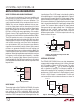
into your processor serial port. The 14-bit serial data will
be received right justified, in a 16-bit word with 16 or
more clocks per frame sync. It is good practice to drive
the LTC2356-12/LTC2356-14 SCK input first to avoid digi-
tal noise interference during the internal bit comparison
decision by the internal high speed comparator. Unlike the
CONV input, the SCK input is not sensitive to jitter because
the input signal is already sampled and held constant.
Serial Data Output (SDO)
Upon power-up, the SDO output is automatically reset to
the high impedance state. The SDO output remains in high
impedance until a new conversion is started. SDO sends
out 12/14 bits in 2’s complement format in the output data
stream beginning at the third rising edge of SCK after the
rising edge of CONV. SDO is always in high impedance
mode when it is not sending out data bits. Please note
the delay specification from SCK to a valid SDO. SDO is
always guaranteed to be valid by the next rising edge of
SCK. The 16-bit output data stream is compatible with the
16-bit or 32-bit serial port of most processors.
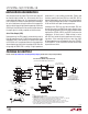
Loading on the SDO line must be minimized. SDO can
directly drive most fast CMOS logic inputs directly. How-
ever, the general purpose I/O pins on many programmable
logic devices (FPGAs, CPLDs) and DSPs have excessive
capacitance. In these cases, a 100Ω resistor in series
with SDO can isolate the input capacitance of the receiv-
ing device. If the receiving device has more than 10pF
of input capacitance or is located far from the LTC2356-
12/LTC2356-14, an NC7SVU04P5X inverter can be used
to provide more drive.
APPLICATIONS INFORMATION
10
1
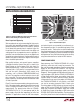
NOTE:
1. DIMENSIONS IN MILLIMETER/(INCH)
2. DRAWING NOT TO SCALE
3. DIMENSION DOES NOT INCLUDE MOLD FLASH, PROTRUSIONS OR GATE BURRS.
MOLD FLASH, PROTRUSIONS OR GATE BURRS SHALL NOT EXCEED 0.152mm (.006") PER SIDE
4. DIMENSION DOES NOT INCLUDE INTERLEAD FLASH OR PROTRUSIONS.
INTERLEAD FLASH OR PROTRUSIONS SHALL NOT EXCEED 0.152mm (.006") PER SIDE
5. LEAD COPLANARITY (BOTTOM OF LEADS AFTER FORMING) SHALL BE 0.102mm (.004") MAX
6. EXPOSED PAD DIMENSION DOES INCLUDE MOLD FLASH. MOLD FLASH ON E-PAD
SHALL NOT EXCEED 0.254mm (.010") PER SIDE.
0.53 ±0.152
(.021 ±.006)
0.18
(.007)
0.254
(.010)
0° – 6° TYP
DETAIL “A”
DETAIL “A”
GAUGE PLANE
5.23
(.206)
MIN
3.20 – 3.45
(.126 – .136)
0.889 ±0.127
(.035 ±.005)
RECOMMENDED SOLDER PAD LAYOUT
1.68 ±0.102
(.066 ±.004)
1.88 ±0.102
(.074 ±.004)
0.50
(.0197)
BSC
0.305 ± 0.038
(.0120 ±.0015)
TYP
BOTTOM VIEW OF
EXPOSED PAD OPTION
1.68
(.066)
1.88
(.074)
1 2
3
4 5
4.90 ±0.152
(.193 ±.006)
0.497 ±0.076
(.0196 ±.003)
REF
8910
7
6
3.00 ±0.102
(.118 ±.004)
(NOTE 3)
3.00 ±0.102
(.118 ±.004)
(NOTE 4)
MSOP (MSE) 0911 REV H
SEATING
PLANE
1.10
(.043)
MAX
0.17 –0.27
(.007 – .011)
TYP
0.86
(.034)
REF
0.50
(.0197)
BSC
0.1016 ±0.0508
(.004 ±.002)
DETAIL “B”
DETAIL “B”
CORNER TAIL IS PART OF
THE LEADFRAME FEATURE.
FOR REFERENCE ONLY
NO MEASUREMENT PURPOSE
0.05 REF
0.29
REF
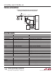
MSE Package
10-Lead Plastic MSOP, Exposed Die Pad
(Reference LTC DWG # 05-08-1664 Rev H)
Please refer to http://www.linear.com/designtools/packaging/ for the most recent package drawings.