
Datasheet

LTC2369-18
10
236918fa
OVERVIEW
The LTC2369-18 is a low noise, low power, high speed 18-bit
successive approximation register (SAR) ADC. Operating
from a single 2.5V supply, the LTC2369-18 supports a
0V to V
REF
pseudo-differential unipolar input range with
V
REF
ranging from 2.5V to 5.1V, making it ideal for high
performance applications which require a wide dynamic
range. The LTC2369-18 achieves ±2.5LSB INL max, no
missing codes at 18 bits and 96.5dB SNR.
Fast 1.6Msps throughput with no cycle latency makes
the LTC2369-18 ideally suited for a wide variety of high
speed applications. An internal oscillator sets the con-
version time, easing external timing considerations. The
LTC2369-18 dissipates only 18mW at 1.6Msps, while an
auto power-down feature is provided to further reduce
power dissipation during inactive periods.
CONVERTER OPERATION
The LTC2369-18 operates in two phases. During the ac-
quisition phase, the charge redistribution capacitor D/A
converter (CDAC) is connected to the IN
+
and IN
–
pins to
sample the pseudo-differential analog input voltage. A ris-
ing edge on the CNV pin initiates a conversion. During the
conversion phase, the 18-bit CDAC is sequenced through a
successive approximation algorithm, effectively comparing
the sampled input with binary-weighted fractions of the
reference voltage (e.g. V
REF
/2, V
REF
/4 … V
REF
/262144)
using the differential comparator. At the end of conver-
sion, the CDAC output approximates the sampled analog
input. The ADC control logic then prepares the 18-bit
digital output code for serial transfer.
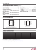
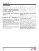
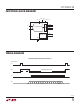
TRANSFER FUNCTION
The LTC2369-18 digitizes the full-scale voltage of REF
into 2
18
levels, resulting in an LSB size of 19μV with
REF = 5V. The ideal transfer function is shown in Figure2.
The output data is in straight binary format.
APPLICATIONS INFORMATION
Figure 2. LTC2369-18 Transfer Function
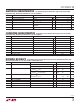
Figure 3. The Equivalent Circuit for the
Differential Analog Input of the LTC2369-18
ANALOG INPUT
The analog inputs of the LTC2369-18 are pseudo-differential
in order to reduce any unwanted signal that is common
to both inputs. The analog inputs can be modeled by the
equivalent circuit shown in Figure 3. The diodes at the input
provide ESD protection. In the acquisition phase, each
input sees approximately 45pF (C
IN
) from the sampling
CDAC in series with 40Ω (R
ON
) from the on-resistance
of the sampling switch. The IN
+
input draws a current
spike while charging the C
IN
capacitor during acquisition.
During conversion, the analog inputs draw only a small
leakage current.
INPUT VOLTAGE (V)
0V
OUTPUT CODE
236918 F02
111...111
111...110
111...101
111...100
000...001
000...000
000...010
000...011
1
LSB
UNIPOLAR
ZERO
FS – 1LSB
1LSB = FS/262144
R
ON
40Ω
C
IN
45pF
R
ON
40Ω
REF
REF
C
IN
45pF
IN
+
IN
–
BIAS
VOLTAGE
236918 F03