
Datasheet
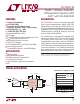

LTC2369-18
4
236918fa
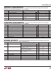
ADC TIMING CHARACTERISTICS
SYMBOL PARAMETER CONDITIONS MIN TYP MAX UNITS
f
SMPL
Maximum Sampling Frequency
l
1.6 Msps
t
CONV
Conversion Time
l
360 412 ns
t
ACQ
Acquisition Time t
ACQ
= t
CYC
– t
CONV
– t
BUSYLH
(Note 10)
l
200 ns
t
CYC
Time Between Conversions
l
625 ns
t
CNVH
CNV High Time
l
20 ns
t
BUSYLH
CNV↑ to BUSY Delay
C
L
= 20pF
l
13 ns
t
CNVL
Minimum Low Time for CNV (Note 11)
l
20 ns
t
QUIET
SCK Quiet Time from CNV↑
(Note 10)
l
20 ns
t
SCK
SCK Period (Notes 11, 12)
l
10 ns
t
SCKH
SCK High Time
l
4ns
The l denotes the specifications which apply over the full operating
temperature range, otherwise specifications are at T
A
= 25°C. (Note 4)
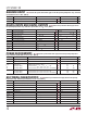
POWER REQUIREMENTS
SYMBOL PARAMETER CONDITIONS MIN TYP MAX UNITS
V
DD
Supply Voltage
l
2.375 2.5 2.625 V
OV
DD
Supply Voltage
l
1.71 5.25 V
I
VDD
I
OVDD
I
PD
I
PD
Supply Current
Supply Current
Power Down Mode
Power Down Mode
1.6Msps Sample Rate
1.6Msps Sample Rate (C
L
= 20pF)
Conversion Done (I
VDD
+ I
OVDD
+ I
REF
, V
REF
> 2V)
Conversion Done (I
VDD
+ I
OVDD
+ I
REF
, V
REF
> 2V, H-Grade)
l
l
l
7.2
0.7
0.9
0.9
8.6
90
140
mA
mA
μA
μA
P
D
Power Dissipation
Power Down Mode
Power Down Mode
1.6Msps Sample Rate
Conversion Done (I
VDD
+ I
OVDD
+ I
REF
, V
REF
> 2V)
Conversion Done (I
VDD
+ I
OVDD
+ I
REF
, V
REF
> 2V, H-Grade)
18
2.25
2.25
21.5
225
315
mW
μW
μW
The l denotes the specifications which apply over the full operating temperature
range, otherwise specifications are at T
A
= 25°C. (Note 4)
REFERENCE INPUT
SYMBOL PARAMETER CONDITIONS MIN TYP MAX UNITS
V
REF
Reference Voltage (Note 5)
l
2.5 5.1 V
I
REF
Reference Input Current (Note 9)
l
0.85 1.1 mA
The l denotes the specifications which apply over the full operating temperature range, otherwise
specifications are at T
A
= 25°C. (Note 4)
DIGITAL INPUTS AND DIGITAL OUTPUTS
SYMBOL PARAMETER CONDITIONS MIN TYP MAX UNITS
V
IH
High Level Input Voltage
l
0.8 • OV
DD
V
V
IL
Low Level Input Voltage
l
0.2 • OV
DD
V
I
IN
Digital Input Current V
IN
= 0V to OV
DD
l
–10 10 μA
C
IN
Digital Input Capacitance 5pF
V
OH
High Level Output Voltage I
O
= –500μA
l
OV
DD
–
0.2 V
V
OL
Low Level Output Voltage I
O
= 500μA
l
0.2 V
I
OZ
Hi-Z Output Leakage Current V
OUT
= 0V to OV
DD
l
–10 10 μA
I
SOURCE
Output Source Current V
OUT
= 0V –10 mA
I
SINK
Output Sink Current V
OUT
= OV
DD
10 mA
The l denotes the specifications which apply over the
full operating temperature range, otherwise specifications are at T
A
= 25°C. (Note 4)