
Datasheet
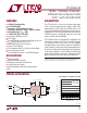

LTC2369-18
8
236918fa
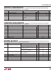
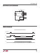
CHAIN (Pin 1): Chain Mode Selector Pin. When low, the
LTC2369-18 operates in normal mode and the RDL/SDI
input pin functions to enable or disable SDO. When high,
the LTC2369-18 operates in chain mode and the RDL/SDI
pin functions as SDI, the daisy-chain serial data input.
Logic levels are determined by OV
DD
.
V
DD
(Pin 2): 2.5V Power Supply. The range of V
DD
is
2.375V to 2.625V. Bypass V
DD
to GND with a 10μF ceramic
capacitor.
GND (Pins 3, 6, 10 and 16): Ground.
IN
+
(Pin 4): Analog Input. IN
+
operates differential with
respect to IN
–
with an IN
+
-IN
–
range of 0V to V
REF
.
IN
–
(Pin 5): Analog Ground Sense. IN
–
has an input range
of ±100mV with respect to GND and must be tied to the
ground plane or a remote ground sense.
REF (Pins 7, 8): Reference Inputs. The range of REF is 2.5V
to 5.1V. This pin is referred to the GND pin and should be
decoupled closely to the pin with a 47μF ceramic capacitor
(X5R, 0805 size).
CNV (Pin 9): Convert Input. A rising edge on this input
powers up the part and initiates a new conversion. Logic
levels are determined by OV
DD
.
BUSY (Pin 11): BUSY Indicator. Goes high at the start of
a new conversion and returns low when the conversion
has finished. Logic levels are determined by OV
DD
.
RDL/SDI (Pin 12): When CHAIN is low, the part is in nor-
mal mode and the pin is treated as a bus enabling input.
When CHAIN is high, the part is in chain mode and the
pin is treated as a serial data input pin where data from
another ADC in the daisy chain is input. Logic levels are
determined by OV
DD
.
SCK (Pin 13): Serial Data Clock Input. When SDO is enabled,
the conversion result or daisy-chain data from another
ADC is shifted out on the rising edges of this clock MSB
first. Logic levels are determined by OV
DD
.
SDO (Pin 14): Serial Data Output. The conversion result
or daisy-chain data is output on this pin on each rising
edge of SCK MSB first. The output data is in straight binary
format. Logic levels are determined by OV
DD
.
OV
DD
(Pin 15): I/O Interface Digital Power. The range of
OV
DD
is 1.71V to 5.25V. This supply is nominally set to
the same supply as the host interface (1.8V, 2.5V, 3.3V,
or 5V). Bypass OV
DD
to GND with a 0.1μF capacitor.
GND (Exposed Pad Pin 17, DFN Package Only): Ground.
Exposed pad must be soldered directly to the ground plane.
PIN FUNCTIONS