
Datasheet

LTC2376-18
13
237618f
–180
AMPLITUDE (dBFS)
–60
–40
–20
–80
–100
–120
–140
–160
0
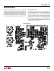
237618 F09b
SNR = 98.4dB
THD = –96.9dB
SINAD = 95.2dB
SFDR = 99.2dB
FREQUENCY (kHz)
0 255075 125100
Figure 9b. 32k Point FFT Plot
with f
IN
= 2kHz for Circuit Shown
in Figure 9a
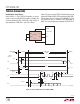
Figure 8. Input Swing of the LTC2376 with Gain
Compression Enabled
APPLICATIONS INFORMATION
positive supply to power the LT6350 results in additional
power savings for the entire system.
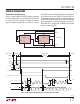
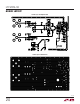
Figure 9a shows how to configure the LT6350 to accept a
±10V true bipolar input signal and attenuate and level shift
the signal to the reduced input range of the LTC2376-18
when digital gain compression is enabled. Figure 9b shows
an FFT plot with the LTC2376-18 being driven by the LT6350
with digital gain compression enabled.
ADC REFERENCE
The LTC2376-18 requires an external reference to define
its input range. A low noise, low temperature drift refer-
ence is critical to achieving the full data sheet performance
of the ADC. Linear Technology offers a portfolio of high
performance references designed to meet the needs of
many applications. With its small size, low power and
high accuracy, the LTC6655-5 is particularly well suited for
use with the LTC2376-18. The LTC6655-5 offers 0.025%
(max) initial accuracy and 2ppm/°C (max) temperature
coefficient for high precision applications. The LTC6655-5
is fully specified over the H-grade temperature range and
complements the extended temperature operation of the
LTC2376-18 up to 125°C. We recommend bypassing the
LTC6655-5 with a 47µF ceramic capacitor (X5R, 0805 size)
close to the REF pin.
The REF pin of the LTC2376-18 draws charge (Q
CONV
) from
the 47µF bypass capacitor during each conversion cycle.
The reference replenishes this charge with a DC current,
I
REF
= Q
CONV
/t
CYC
. The DC current draw of the REF pin,
I
REF
, depends on the sampling rate and output code. If
the LTC2376-18 is used to continuously sample a signal
at a constant rate, the LTC6655-5 will keep the deviation
of the reference voltage over the entire code span to less
than 0.5LSBs.
When idling, the REF pin on the LTC2376-18 draws only
a small leakage current (< 1µA). In applications where a
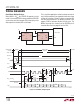
burst of samples is taken after idling for long periods as
shown in Figure 10, I
REF
quickly goes from approximately
CNV
IDLE
PERIOD
IDLE
PERIOD
237618 F10
Figure 10. CNV Waveform Showing Burst Sampling
Figure 9a. LT6350 Configured to Accept a ±10V Input Signal While Running Off of a
Single 5.5V Supply When Digital Gain Compression Is Enabled in the LTC2376-18
237618 F08
5V
4.5V
0.5V
0V
LT6350
3.01k
4.32k
V
CM
237618 F09a
OUT1
R
INT
R
INT
R
IN
= 15k
OUT2
V
–
8
4
5
2
1
6
V
+
3
+
–
–
+
20
3300pF
20
6.04k
1k
V
CM
1k
0.5V
4.5V
0.5V
4.5V
5V
5.5V
47µF
10µF
10µF
LTC2376-18
REF/DGC
IN
+
REF V
DD
2.5V
IN
–
LTC6655-5V
IN
V
OUT_S
V
OUT_F
–10V
10V
0V
6800pF
6800pF