
Datasheet

LTC2376-18
19
237618f
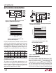
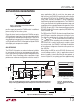
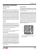
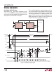
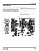
BOARD LAYOUT
To obtain the best performance from the LTC2376-18
a printed circuit board is recommended. Layout for the
printed circuit board (PCB) should ensure the digital and
analog signal lines are separated as much as possible. In
particular, care should be taken not to run any digital clocks
or signals alongside analog signals or underneath the ADC.
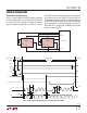
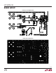
Recommended Layout
The following is an example of a recommended PCB layout.
A single solid ground plane is used. Bypass capacitors to
the supplies are placed as close as possible to the supply
pins. Low impedance common returns for these bypass
capacitors are essential to the low noise operation of the
ADC. The analog input traces are screened by ground.
For more details and information refer to DC1783A, the
evaluation kit for the LTC2376-18.
Partial Top Silkscreen