
Datasheet


LTC2377-20
12
237720f
For more information www.linear.com/LTC2377-20
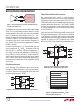
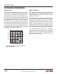
ing temperature range and common mode input voltage
range. Thus, any reasonable mismatch (below 5%) of the
source impedances R
S1
and R
S2
will cause only a negligible
error. The differential input leakage current, (I
L1
– I
L2
),
depends on temperature and is maximum when V
IN
= V
REF
,
as shown in Figure 6. The differential leakage current is
also typically very small, and its nonlinear component is
even smaller. Only the nonlinear component will impact
the ADC’s linearity.
For optimal performance, it is recommended that the
source impedances, R
S1
and R
S2
, be between 10Ω and
50Ω and with 1% tolerance. For source impedances in
this range, the voltage and temperature coefficients of
R
S1
and R
S2
are usually not critical. The guaranteed AC
and DC specifications are tested with 10Ω source imped-
ances, and the specifications will gradually degrade with
increased source impedances due to incomplete settling
of the inputs.
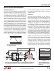
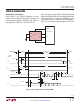
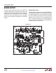
Fully Differential Inputs
A low distortion fully differential signal source driven
through the LT6203 configured as two unity gain buffers
as shown in Figure 8 can be used to get the full data sheet
distortion performance of –125dB.
applicaTions inForMaTion
Single-Ended-to-Differential Conversion
For single-ended input signals, a single-ended-t
o-
differential conversion circuit must be used to produce
a differential signal at the inputs of the LTC2377-20. The
LT6203 ADC driver is recommended for performing single-
ended-to-differential conversions. The LT6203 is flexible
and may be configured to convert single-ended signals
of various amplitudes to the ±5V differential input range
of the LTC2377-20.
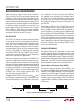
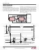
Figure 9a shows the LT6203 being used to convert a 0V to
5V single-ended input signal. In this case, the first amplifier
is configured as a unity gain buffer and the single-ended
input signal directly drives the high-impedance input of the
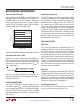
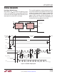
amplifier. As shown in the FFT of Figure 9b, the LT6203
drives the LTC2377-20 to near full data sheet performance.
LT6203
V
CM
= REF/2
237720 F09a
0V
5V
0V
5V
OUT2
499Ω 499Ω
249Ω
OUT1
3
7
1
5
6
2
+
–
+
–
–
+
0V
5V
10µF
FREQUENCY (kHz)
0 50 100 150 200 250
–180
AMPLITUDE (dBFS)
–60
–40
–20
–80
–100
–120
–140
–160
0
237720 F09b
SNR = 104dB
THD = –121.1dB
SINAD = 103.9dB
SFDR = 122.9dB
Figure 9a. LT6203 Converting a 0V to 5V Single-
Ended Signal to a ±5V Differential Input Signal
Figure9b. 128k Point FFT Plot with f
IN
= 2kHz
for Circuit Shown in Figure 9a
Figure 8. LT6203 Buffering a Fully Differential Signal Source
LT6203
237720 F08
0V
5V
0V
5V
5
7
6
+
–
0V
5V
3
1
2
+
–
0V
5V
Figure 7. Source Impedances of a Driver and Input Leakage
Currents of the LTC2377-20
R
S1
R
S2
I
L1
I
L2
237720 F07
IN
+
V
E
IN
–
+
–
LTC2377-20