
Datasheet


LTC2383-16
12
238316f
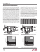
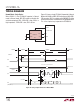
The LT6350 can also be used to buffer and convert single-
ended signals larger than the input range of the LTC2383-16
in order to maximize the signal swing that can be digitized.
Figure 6 shows the LT6350 converting a 0V-5V single-ended
input signal to the ±2.5V differential input range of the
LTC2383-16. In this case, the first amplifier in the LT6350
is configured as an inverting amplifier stage, which acts to
attenuate the input signal down to the 0V-2.5V input range
of the LTC2383-16. In the inverting amplifier configuration,
the single-ended input signal source no longer directly
drives a high impedance input of the first amplifier. The
input impedance is instead set by resistor R
IN
. R
IN
must
be chosen carefully based on the source impedance of the
signal source. Higher values of R
IN
tend to degrade both
the noise and distortion of the LT6350 and LTC2383-16 as a
system. R1, R2 and R3 must be selected in relation to R
IN
to
achieve the desired attenuation and to maintain a balanced
input impedance in the first amplifier. Table 1 shows the
APPLICATIONS INFORMATION
LT6350
R1 = 1k
R2 = 1k
R3 = 2k
R4 = 665
V
CM
= V
REF
/2
V
REF
75pF
150pF
0V to
2.5V
2.5V to
0V
0V to 5V
238316 F06
OUT1
R
INT
10
µF
R
INT
R
IN
= 2k
OUT2
8
4
5
2
1
+
–
+
–
–
+
Figure 6. LT6350 Converting a 0V-5V Single-Ended Signal to
a ±2.5V Differential Input Signal
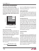
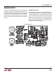
Figure 6a. 32k Point FFT Plot for Circuit Shown in Figure 6
LT6350
R1 = 1.24k
R2 = 1.24k
R3 = 10k
R4 = 1.1k
V
CM
= V
REF
/2
V
CM
0V to
2.5V
2.5V to
0V
±10V
238316 F07
OUT1
R
INT
R
INT
R
IN
= 10k
OUT2
8
4
5
2
1
+
–
+
–
–
+
220pF
10µF
200pF
resulting SNR and THD for several values of R
IN
, R1, R2
and R3 in this configuration. Figure 6a shows the resulting
FFT when using the LT6350 as shown in Figure 6.
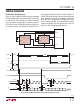
The LT6350 can also be used to buffer and convert large,
true bipolar signals which swing below ground to the ±2.5V
differential input range of the LTC2383-16. Figure 7 shows
the LT6350 being used to convert a ±10V true bipolar signal
for use by the LTC2383-16. The input impedance is again
set by resistor R
IN
. Table 2 shows the resulting SNR and
THD for several values of R
IN
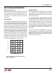
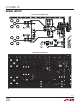
. Figure 7a shows the resulting
FFT when using the LT6350 as shown in Figure 7.
Table 1. SNR, THD vs R
IN
for 0-5V Single-Ended Input Signal.
R
IN
(Ω)
R1
(Ω)
R2
(Ω)
R3
(Ω)
R4
(Ω)
SNR
(dB)
THD
(dB)
2k 1k 1k 2k 665 92 –101
10k 5k 5k 10k 3.3k 91 –100
100k 50k 50k 100k 16k 91 –94
Figure 7. LT6350 Converting a ±10V Single-Ended Signal to
a ±2.5V Differential Input Signal
Figure 7a. 32k Point FFT Plot for Circuit Shown in Figure 7
FREQUENCY (kHz)
0 100 200 300 400 500
–180
AMPLITUDE (dBFS)
–60
–40
–20
–80
–100
–120
–140
–160
0
238316 F06a
SNR = 92dB
THD = –101dB
SINAD = 91.4dB
SFDR = 103dB
FREQUENCY (kHz)
0 100 200 300 400 500
–180
AMPLITUDE (dBFS)
–60
–40
–20
–80
–100
–120
–140
–160
0
238316 F07a
SNR = 92dB
THD = –97dB
SINAD = 91.2dB
SFDR = 99.7dB