
Datasheet


LTC2383-16
8
238316f
CHAIN (Pin 1): Chain Mode Selector Pin. When low, the
LTC2383-16 operates in Normal Mode and the RDL/SDI
input pin functions to enable or disable SDO. When high,
the LTC2383-16 operates in Chain Mode and the RDL/SDI
pin functions as SDI, the daisychain serial data input.
V
DD
(Pin 2): 2.5V Digital Power Supply. The range of
V
DD
is 2.375V to 2.625V. Bypass V
DD
to GND with a 10µF
ceramic capacitor.
GND (Pins 3, 6, 10 and 16): Ground.
IN
+
, IN
–
(Pins 4, 5): Positive and Negative Differential
Analog Inputs.
REF (Pins 7, 8): Reference Input. The range of REF is 2.4V
to 2.6V. This pin is referred to the GND pin and should be
decoupled closely to the pin with a 47µF ceramic capacitor
(X5R, 0805 size).
CNV (Pin 9): Convert Input. A rising edge on this input
initiates a new conversion. When the conversion is done,
the part powers down as long as CNV is held high. When
CNV is returned low, the part powers up in preparation
for the next conversion.
BUSY (Pin 11): BUSY indicator. Goes high at the start of
a new conversion and returns low when the conversion
has finished.
RDL/SDI (Pin 12): When CHAIN is low, the part is in Normal
Mode and the pin is treated as a bus enabling input. When
CHAIN is high, the part is in chain mode and the pin is
treated as a serial data input pin where data from another
ADC in the daisychain is input.
SCK (Pin 13): Serial Data Clock Input. When SDO is enabled,
the conversion result or daisychain data from another ADC
is shifted out on the rising edges of this clock MSB first.
SDO (Pin 14): Serial Data Output. The conversion result or
daisychain data is output on this pin on each rising edge
of SCK MSB first. The output data is in 2’s complement
format.
OV
DD
(Pin 15): I/O Interface Digital Power. The range of
OV
DD
is 1.71V to 5.25V. This supply is nominally set to
the same supply as the host interface (1.8V, 2.5V, 3.3V,
or 5V). Bypass OV
DD
to GND with a 0.1µF capacitor.
GND (Exposed Pad Pin 17 – DFN Package Only): Ground.
Exposed pad must be soldered directly to the ground
plane.
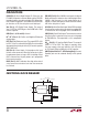
FUNCTIONAL BLOCK DIAGRAM
PIN FUNCTIONS
REF = 2.5V
LTC2383-16
IN
+
V
DD
= 2.5V
OV
DD
= 1.8V to 5V
IN
–
CHAIN
CNV
GND
BUSY
SDO
SCK
RDL/SDI
CONTROL LOGIC
16-BIT SAMPLING ADC
SPI
PORT
+
–
238316 BD01