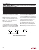
LTC2389-16 16-Bit, 2.5Msps SAR ADC with Pin-Configurable Analog Input Range and 96dB SNR Description Features n n n n n n n n n n n n n n 2.5Msps Throughput Rate ±1LSB INL (Max) Guaranteed 16-Bit, No Missing Codes Pin-Configurable Analog Input Range: ±4.096V Fully Differential 0V to 4.096V Pseudo-Differential Unipolar ±2.048V Pseudo-Differential Bipolar 96.0dB (Fully Differential)/93.
LTC2389-16 Absolute Maximum Ratings (Notes 1, 2) Supply Voltage (VDD , OVDD)........................................6V Analog Input Voltage (Note 3) IN+, IN–, REFIN, CNVST......(GND – 0.3V) to (VDD + 0.3V) Digital Input Voltage (Note 3)........................... (GND – 0.3V) to (OVDD + 0.3V) Digital Output Voltage (Note 3)........................... (GND – 0.3V) to (OVDD + 0.3V) Power Dissipation............................................... 500mW Operating Temperature Range LTC2389C.....................
LTC2389-16 Analog Input The l denotes the specifications which apply over the full operating temperature range, otherwise specifications are at TA = 25°C. (Note 4) SYMBOL PARAMETER CONDITIONS VIN+ Absolute Input Range (IN+) MIN TYP (Note 5) l –0.1 VREF + 0.1 V VIN– Absolute Input Range (IN–) Fully Differential (Note 5) Pseudo-Differential Unipolar (Note 5) Pseudo-Differential Bipolar (Note 5) l l l –0.1 –0.1 VREF /2 – 0.1 VREF + 0.1 0.1 VREF /2 + 0.
LTC2389-16 Dynamic Accuracy The l denotes the specifications which apply over the full operating temperature range, otherwise specifications are at TA = 25°C. AIN = –1dBFS (Notes 4, 8) SYMBOL PARAMETER CONDITIONS SINAD Signal-to-(Noise + Distortion) Ratio Fully Differential, fIN = 2kHz Pseudo-Differential Unipolar, fIN = 2kHz Pseudo-Differential Bipolar, fIN = 2kHz SNR THD SFDR MIN TYP l l l 94.4 91.2 91.7 96.0 93.2 93.
LTC2389-16 Digital Inputs And Digital Outputs The l denotes the specifications which apply over the full operating temperature range, otherwise specifications are at TA = 25°C.
LTC2389-16 Timing Characteristics The l denotes the specifications which apply over the full operating temperature range, otherwise specifications are at TA = 25°C.
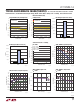
LTC2389-16 Typical Performance Characteristics TA = 25°C, VDD = 5V, OVDD = 2.5V, VREF = 4.096V External Reference, Fully Differential Range (PD/FD = 0V), VCM = 2.048V, fSMPL = 2.5Msps, unless otherwise noted. 0.5 INTERNAL REF EXTERNAL REF 0.4 0.2 0.2 0 –0.2 –0.4 –0.2 –0.4 49152 OUTPUT CODE –0.5 65536 40000 0 16384 238916 G01 240000 4.096 REFERENCE OUTPUT (V) 4.097 200000 COUNTS 160000 120000 80000 40000 32768 49152 0 65536 0 32762 32763 32764 CODE 32765 32766 4.095 4.094 4.
LTC2389-16 Typical Performance Characteristics TA = 25°C, VDD = 5V, OVDD = 2.5V, VREF = 4.096V External Reference, Fully Differential Range (PD/FD = 0V), VCM = 2.048V, fSMPL = 2.5Msps, unless otherwise noted. THD, Harmonics vs Temperature, fIN = 2kHz –110 97 –115 96 SINAD SNR 95 INL/DNL vs Temperature 1.
LTC2389-16 Typical Performance Characteristics TA = 25°C, VDD = 5V, OVDD = 2.5V, VREF = 4.096V External Reference, Pseudo-Differential Unipolar Range (PD/FD = OVDD, OB/2C = OVDD), fSMPL = 2.5Msps, unless otherwise noted. Differential Nonlinearity vs Output Code Integral Nonlinearity vs Output Code INTERNAL REF EXTERNAL REF 0.8 0.6 0.3 0.4 0.2 0.2 0 –0.2 –0.4 49152 OUTPUT CODE –0.5 65536 80000 –0.2 –0.3 32768 120000 0 –0.4 16384 160000 –0.1 –0.8 0 200000 0.1 –0.
LTC2389-16 Typical Performance Characteristics TA = 25°C, VDD = 5V, OVDD = 2.5V, VREF = 4.096V External Reference, Pseudo-Differential Unipolar Range (PD/FD = OVDD, OB/2C = OVDD), fSMPL = 2.5Msps, unless otherwise noted. –115 Offset Error vs Temperature 1.0 THD 2ND –120 –125 3RD 0.5 MAX INL OFFSET ERROR (LSB) THD, HARMONICS (dB) –110 INL/DNL vs Temperature 1.0 INL/ DNL ERROR (LSB) –105 THD, Harmonics vs Temperature, fIN = 2kHz MAX DNL 0 MIN DNL MIN INL –0.5 0.5 0 –0.
LTC2389-16 Typical Performance Characteristics TA = 25°C, VDD = 5V, OVDD = 2.5V, VREF = 4.096V External Reference, Pseudo-Differential Bipolar Range (PD/FD = OVDD, OB/2C = OV), fSMPL = 2.5Msps, unless otherwise noted. Integral Nonlinearity vs Output Code INTERNAL REF EXTERNAL REF 0.8 0.6 0.3 0.4 0.2 0.2 0 –0.2 –0.4 49152 OUTPUT CODE –0.
LTC2389-16 Typical Performance Characteristics TA = 25°C, VDD = 5V, OVDD = 2.5V, VREF = 4.096V External Reference, Pseudo-Differential Bipolar Range (PD/FD = OVDD, OB/2C = OV), fSMPL = 2.5Msps, unless otherwise noted. 2ND –120 –125 –130 –135 –55 –35 –15 0.5 MAX INL OFFSET ERROR (LSB) THD, HARMONICS (dB) Offset Error vs Temperature 1.0 THD –110 –115 INL/DNL vs Temperature 1.0 INL/ DNL ERROR (LSB) –105 THD, Harmonics vs Temperature, fIN = 2kHz MAX DNL 0 MIN DNL MIN INL –0.5 0.5 0 –0.
LTC2389-16 Pin Functions GND (Pins 1, 17, 20, 35, 41, 44, 48, Exposed Pad Pin 49 (QFN Only)): Ground. Solder all GND pins and exposed pad to the ground plane. VDD (Pins 2, 3, 19, 40, 45, 46, 47): 5V Power Supply. The range of VDD is 4.75V to 5.25V. Bypass VDD network to GND with a 0.1μF ceramic capacitor close to each pin and a 10μF ceramic capacitor in parallel. MODE0 (Pin 4): Data Bus Configuration Input.
LTC2389-16 Pin Functions is the serial data input, which can be used to daisy chain two or more converters on a single SDO line. The digital data level on SDI is output on SDO with a delay of 16 SCK periods after the start of the read sequence. Logic levels are determined by OVDD. D10/SDO (Pin 23): Data Bit 10/Serial Data Output. When MODE0 = 0, this pin is bit 10 of the parallel data output bus, as described in Table 1.
LTC2389-16 Pin Functions PD/FD (Pin 30): Pseudo-Differential/Fully-Differential Input. This pin, in conjunction with Pin 6 (OB/2C), controls the analog input range of the converter and the binary format of the conversion result, as described in Table 2. Logic levels are determined by OVDD. CS (Pin 31): Chip Select Input. The data I/O bus is enabled when CS is low and goes Hi-Z when CS is high. CS also gates the external shift clock. Logic levels are determined by OVDD. RESET (Pin 32): Reset Input.
LTC2389-16 FUNCTIONAL Block Diagram VDD OVDD LTC2389-16 16-BIT OR 8-BIT BUS SDI SDO IN+ 16-BIT SAMPLING ADC IN– 16 BITS PARALLEL/ SERIAL INTERFACE SCK CS MODE1 1x BUFFER MODE0 REFIN A1 A0 REFOUT VCM 4.
LTC2389-16 Timing Diagrams Conversion Timing Using the Parallel Interface CS = RESET = 0 CNVST CONVERT BUSY D[15:0] ACQUIRE PREVIOUS CONVERSION CURRENT CONVERSION Conversion Timing Using the Serial Interface CS = RESET = 0 CNVST BUSY CONVERT SCK SDO ACQUIRE 1 DON’T CARE 2 3 4 5 6 7 8 9 10 11 12 13 14 15 16 D15 D14 D13 D12 D11 D10 D9 D8 D7 D6 D5 D4 D3 D2 D1 D0 238916 TD01 238916f 17
LTC2389-16 Applications Information TRANSFER FUNCTION The LTC2389-16 is a low noise, high speed 16-bit successive approximation register (SAR) ADC. Operating from a single 5V supply, the LTC2389-16 supports pin-configurable fully differential (±4.096V), pseudo-differential unipolar (0V to 4.096V) and pseudo-differential bipolar (±2.048V) analog input ranges, allowing it to interface with multiple signal chain formats without requiring additional level translation or signal conditioning.
LTC2389-16 Applications Information ANALOG INPUT Pseudo-Differential Unipolar Input Range The analog inputs of the LTC2389-16 can be pin configured to accept one of three input voltage ranges: fully differential (±4.096V), pseudo-differential unipolar (0V to 4.096V), and pseudo-differential bipolar (±2.048V).
LTC2389-16 Applications Information Input Filtering The noise and distortion of the buffer amplifier and other supporting circuitry must be considered since they add to the ADC noise and distortion. A buffer amplifier with low noise density must be selected to minimize SNR degradation. A filter network should be placed between the buffer output and ADC input to both minimize the noise contribution of the buffer and reduce disturbances reflected into the buffer from ADC sampling transients.
LTC2389-16 Applications Information 4.096V 0V LOWPASS FILTERS 1/2 LT6201 0V – + 4.096V 10Ω 49.9Ω IN+ 1nF 0V 4.096V LTC2389-16 + – 0V 4.096V 10Ω 1nF 49.9Ω IN– 238916 F05a 1/2 LT6201 0V 2.048V Figure 5a. LT6201 Buffering a Fully-Differential or Single-Ended Signal Source 0 SNR = 93.2dB –20 THD = –112dB SINAD = 93.2dB –40 SFDR = 113dB –60 –80 –100 –120 0 SNR = 93.5dB –20 THD = –111dB SINAD = 93.5dB –40 SFDR = 112dB AMPLITUDE (dBFS) AMPLITUDE (dBFS) AMPLITUDE (dBFS) 0 SNR = 96.
LTC2389-16 Applications Information In applications where slightly degraded SNR and THD performance is acceptable, it is possible to drive the LTC2389-16 using the lower power LT6231 ADC driver configured as two unity-gain buffers, as shown in Figure 6a. The RC time constant of the output lowpass filter is larger in this topology to limit the high frequency noise contribution of the LT6231. As shown in the FFT plots in Figures 6b-6d, this circuit achieves 95.
LTC2389-16 Applications Information Single-Ended to Differential Conversion In some applications it may be desirable to convert a single-ended unipolar or bipolar signal to a fully-differential signal prior to driving the LTC2389-16 to take advantage of the higher SNR of the LTC2389-16 in fully differential input mode. The LT6201 ADC driver configured in the topology shown in Figure 7a can be used to convert a 0V to 4.096V single-ended input signal to a fully-differential ±4.096V output signal.
LTC2389-16 Applications Information An alternate single-ended to differential topology employing the LT6231 followed by the LT6201 is shown in Figure 8a. This topology enables additional band-limiting of the wideband noise of the single-ended to differential 4.096V 4.096V 0V + – 1/2 LT6231 LOWPASS FILTERS A 0V 1k 50Ω VCM = 2.048V LOWPASS FILTERS B 49.
LTC2389-16 Applications Information Single-Ended Unipolar and Bipolar Inputs LT6200 combines fast settling and good DC linearity with a 0.95nV/√Hz input-referred noise density, enabling it to achieve the full ADC data sheet SNR and THD specifications in both pseudo-differential input modes, as shown in the FFT plots in Figures 9b and 9c. The LTC2389-16 accepts both single-ended unipolar and single-ended bipolar input signals directly.
LTC2389-16 Applications Information In applications where slightly degraded SNR and THD performance is acceptable, it is possible to drive the LTC2389-16 using the lower power LT6230 ADC driver configured as a unity-gain buffer, as shown in Figure 10a. The RC time constant of the output lowpass filter is larger in this topology to limit the high frequency noise contribution of the LT6230. As shown in the FFT plots in Figures 10b and 10c, this circuit achieves 92.
LTC2389-16 Applications Information ADC REFERENCE DYNAMIC PERFORMANCE A low noise, low temperature drift reference is critical to achieving the full data sheet performance of the ADC. The LTC2389-16 provides an excellent internal reference with a ±20ppm/°C (maximum) temperature coefficient. If even better accuracy is required, an external reference can be used. In both cases, the high speed, low noise internal reference buffer is employed and cannot be bypassed.
LTC2389-16 Applications Information Total Harmonic Distortion (THD) Power Supply Sequencing Total harmonic distortion (THD) is the ratio of the RMS sum of all harmonics of the input signal to the fundamental itself. The out-of-band harmonics alias into the frequency band between DC and half the sampling frequency (fSMPL /2). THD is expressed as: The LTC2389-16 does not have any specific power supply sequencing requirements.
LTC2389-16 Applications Information Power Shutdown Mode When PD is tied high, the LTC2389-16 enters power shutdown. In this state, all internal functions, including the reference, are turned off and subsequent conversion requests are ignored. Before entering power shutdown, the digital output data should be read.
LTC2389-16 Applications Information DIGITAL INTERFACE 8-Bit Parallel Bus Configuration To accommodate a variety of application-specific processor and FPGA data bus widths, the LTC2389-16 output bus may be configured to operate in either 16-bit parallel, 8-bit parallel or serial modes, as described in Table 1. The flexible OVDD supply allows the LTC2389-16 to communicate with any digital logic operating between 1.8V and 5V, including 2.5V and 3.3V systems.
LTC2389-16 Applications Information MODE0 = 0, A1 = 0, MODE1 = A0 = 0 tCNVSTL CS = 0, MODE0 = 0, A1 = 0, MODE1 = A0 = 0 CNVST, CS tCNVSTL CNVST BUSY BUSY tCONV tBUSYLH DATA BUS D[15:0] tCONV tBUSYLH tDDBUSYL CURRENT CONVERSION PREVIOUS CONVERSION DATA BUS D[15:0] Hi-Z 238916 F14 Figure 16. Read the Parallel Data During the Following Conversion MODE0 = 0, MODE1 = A0 = 0 MODE0 = 0, A1 = 0, MODE1 = A0 = 0 CS CS BUSY A1 Hi-Z CURRENT CONVERSION tEN 238916 F16 tDIS tEN Figure 14.
LTC2389-16 Applications Information SCK STARTS LOW MODE0 = 1, A1 = X, MODE1 = A0 = 0 tDSCK CS BUSY tSCK tSCKL tSCKH SCK 1 2 4 3 15 16 17 18 tDSDO, tHSDO SDO (ADC 2) Hi-Z tEN D13 D1 D0 X15 X14 tHSDI tSSDI SDI (ADC 2) D14 D15 Hi-Z X15 X14 X13 X1 X0 SCK STARTS HIGH MODE0 = 1, A1 = X, MODE1 = A0 = 0 tDSCK CS BUSY tSCK tSCKL tSCKH SCK 1 2 3 4 15 16 17 18 tDSDO, tHSDO SDO (ADC 2) Hi-Z D15 tEN tSSDI SDI (ADC 2) Hi-Z D14 D13 D1 D0 X15 X14 tHSDI X15 X14 X13
LTC2389-16 Applications Information Serial Bus Configuration In applications where a serial bus is required to minimize the data bus width, the LTC2389-16 is capable of providing each conversion result R[15:0] serially on pin D10/ SDO. To select this bus configuration, pin MODE0 should be driven to MODE0 = 1, as described in Table 1. Address input pin A1 has no effect on the parsing or presentation of serial conversion data.
LTC2389-16 Applications Information BOARD LAYOUT To obtain the best performance from the LTC2389-16, a printed circuit board (PCB) is recommended. Layout for the printed circuit board should ensure the digital and analog signal lines are separated as much as possible. In particular, care should be taken not to run any digital clocks or signals alongside analog signals or underneath the ADC. and 8 (A1).
LTC2389-16 Applications Information 238916 F21 Partial Layer 1 Component Side 238916 F22 Partial Layer 2 Ground Plane 238916f 35
LTC2389-16 Applications Information 238916 F23 Partial Layer 3 Power Plane 238916 F24 Partial Layer 4 Bottom Layer 238916 F25 Bottom Silk Partial 238916f 36
AIN0V - 4.096V AIN+ 0V - 4.096V CLK 100MHz MAX 3.3VPP J3 J2 0 Ohm R41 -IN JP2 0 Ohm R14 +IN JP1 0.1uF R6 49.9 1% 1206 C5 AC AC DC R4 1K R2 1K C12 DC 10uF C16 (OPT) 10uF C32 (OPT) C31 2 3 5 4 C2 0.1uF (OPT) C17 R42 (OPT) R40 (OPT) INT JP3 EXT CM C33 (OPT) C30 10uF 330pF 402 1% C25 R29 VCMX2 R19 (OPT) R11 (OPT) C10 10uF U3 NC7SZ04P5X VCMX2 C41 10uF C40 0.
LTC2389-16 Package Description Please refer to http://www.linear.com/designtools/packaging/ for the most recent package drawings. LX Package 48-Lead Plastic LQFP (7mm × 7mm) (Reference LTC DWG # 05-08-1760 Rev Ø) 7.15 – 7.25 9.00 BSC 5.50 REF 7.00 BSC 48 0.50 BSC 1 2 48 SEE NOTE: 4 1 2 9.00 BSC 5.50 REF 7.00 BSC 7.15 – 7.25 0.20 – 0.30 A A PACKAGE OUTLINE C0.30 – 0.50 1.30 MIN RECOMMENDED SOLDER PAD LAYOUT APPLY SOLDER MASK TO AREAS THAT ARE NOT SOLDERED 1.60 1.35 – 1.45 MAX 11° – 13° R0.
LTC2389-16 Package Description Please refer to http://www.linear.com/designtools/packaging/ for the most recent package drawings. UK Package 48-Lead Plastic QFN (7mm × 7mm) (Reference LTC DWG # 05-08-1704) 0.70 ±0.05 5.15 ± 0.05 5.50 REF 6.10 ±0.05 7.50 ±0.05 (4 SIDES) 5.15 ± 0.05 PACKAGE OUTLINE 0.25 ±0.05 0.50 BSC RECOMMENDED SOLDER PAD PITCH AND DIMENSIONS APPLY SOLDER MASK TO AREAS THAT ARE NOT SOLDERED 7.00 ± 0.10 (4 SIDES) 0.75 ± 0.05 R = 0.10 TYP R = 0.115 TYP 47 48 0.40 ± 0.
LTC2389-16 Typical Application ADC Driver: Single-Ended Input to Differential Output 4.096V 4.096V 0V + – 1/2 LT6201 0V 330pF 49.9Ω 10Ω 330pF 402Ω 1nF IN+ 1nF IN– LTC2389-16 402Ω 1/2 LT6201 + – LOWPASS FILTERS – + 10Ω 49.9Ω 238916 TA02 4.096V VCM = 2.048V 0V Related Parts PART NUMBER DESCRIPTION COMMENTS 18-Bit, 2.5Msps, All-In-One ADC 5V Supply, Pin-Configurable Input, 99.8dB SNR, ±4.096V, 0V to 4.096V, and ±2.048V Input Ranges, Internal 4.