
Datasheet


LTC2389-16
26
238916f
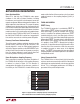
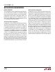
In applications where slightly degraded SNR and THD
performance is acceptable, it is possible to drive the
LTC2389-16 using the lower power LT6230 ADC driver
configured as a unity-gain buffer, as shown in Figure10a.
The RC time constant of the output lowpass filter is
larger in this topology to limit the high frequency noise
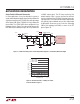
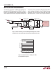
contribution of the LT6230. As shown in the FFT plots in
Figures10b and 10c, this circuit achieves 92.5dB SNR
and –112dB THD in unipolar input mode and 92.8dB SNR
and –111dB THD in bipolar input mode.
Note that in the circuits of Figures 9a and 10a, the source
impedance of the signal applied to IN
–
directly affects input
settling time during signal acquisition. In single-ended
applications where the impedance of this reference signal
is intrinsically high, the dual-buffer approach shown in
Figures 5a and 6a will provide for faster acquisition time
and better distortion performance from the ADC.
Figure 10b. 32k Point FFT f
SMPL
= 2.5Msps, f
IN
= 2kHz, for
Circuit Shown in Figure 10a; Driven with Unipolar Inputs
Figure 10c. 32k Point FFT f
SMPL
= 2.5Msps, f
IN
= 2kHz, for
Circuit Shown in Figure 10a; Driven with Bipolar Inputs
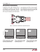
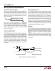
applications inFormation
238916 F10a
IN
–
IN
+
1nF
15Ω
LOWPASS FILTER
LTC2389-16
LT6230
+
–
49.9Ω
49.9Ω
4.096V
0V
0V
4.096V
0V
2.048V
Figure 10a. The LT6230 Buffering a Single-Ended Signal Source
FREQUENCY (kHz)
0
AMPLITUDE (dBFS)
–60
–40
–20
–80
–100
500250 750 1000 1250
–160
–180
–120
0
–140
238916 F10b
SNR = 92.5dB
THD = –112dB
SINAD = 92.5dB
SFDR = 112dB
FREQUENCY (kHz)
0
AMPLITUDE (dBFS)
–60
–40
–20
–80
–100
500250 750 1000 1250
–160
–180
–120
0
–140
238916 F10c
SNR = 92.8dB
THD = –111dB
SINAD = 92.7dB
SFDR = 112dB