
Datasheet


18
LTC2400
APPLICATIONS INFORMATION
WUU
U
Once CS is pulled LOW, SCK goes LOW and EOC is output
to the SDO pin. EOC = 1 while a conversion is in progress
and EOC = 0 if the device is in the sleep state.
When testing EOC, if the conversion is complete (EOC = 0),
the device will exit the sleep state and enter the data output
state if CS remains LOW. In order to prevent the device
from exiting the low power sleep state, CS must be pulled
HIGH before the first rising edge of SCK. In the internal
SCK timing mode, SCK goes HIGH and the device begins
outputting data at time t
EOCtest
after the falling edge of CS
(if EOC = 0) or t
EOCtest
after EOC goes LOW (if CS is LOW
during the falling edge of EOC). The value of t
EOCtest
is 23µs
if the device is using its internal oscillator (F
0
= logic LOW
or HIGH). If F
O
is driven by an external oscillator of
frequency f
EOSC
, then t
EOCtest
is 3.6/f
EOSC
. If CS is pulled
HIGH before time t
EOCtest
, the device remains in the sleep
state. The conversion result is held in the internal static
shift register.
If CS remains LOW longer than t
EOCtest
, the first rising
edge of SCK will occur and the conversion result is serially
shifted out of the SDO pin. The data output cycle begins on
this first rising edge of SCK and concludes after the 32nd
rising edge. Data is shifted out the SDO pin on each falling
edge of SCK. The internally generated serial clock is output
to the SCK pin. This signal may be used to shift the
conversion result into external circuitry. EOC can be
latched on the first rising edge of SCK and the last bit of the
conversion result on the 32nd rising edge of SCK. After the
32nd rising edge, SDO goes HIGH (EOC = 1), SCK stays
HIGH, and a new conversion starts.
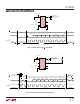
Typically, CS remains LOW during the data output state.
However, the data output state may be aborted by pulling
CS HIGH anytime between the first and 32nd rising edge
of SCK, see Figure 9. On the rising edge of CS, the device
aborts the data output state and immediately initiates a
new conversion. This is useful for systems not requiring
all 32 bits of output data, aborting an invalid conversion
cycle, or synchronizing the start of a conversion. If CS is
pulled HIGH while the converter is driving SCK LOW, the
internal pull-up is not available to restore SCK to a logic
SDO
SCK
(INTERNAL)
CS
>t
EOCtest
MSBEXRSIG
BIT 8
TEST EOCTEST EOC
BIT 27 BIT 26BIT 28BIT 29BIT 30
EOC
BIT 31
EOC
BIT 0
SLEEP DATA OUTPUT
Hi-Z Hi-Z Hi-Z Hi-Z Hi-Z
DATA OUTPUT
CONVERSIONCONVERSIONSLEEP
2400 F09
<t
EOCtest
V
CC
F
O
V
REF
SCK
V
IN
SDO
GND CS
V
REF
0.1V TO V
CC
V
IN
–0.12V
REF
TO 1.12V
REF
1µF
2.7V TO 5.5V
LTC2400
V
CC
10k
= 50Hz REJECTION
= EXTERNAL OSCILLATOR
= 60Hz REJECTION
V
CC
TEST EOC
Figure 9. Internal Serial Clock, Reduced Data Output Length