
Datasheet

LTC2410
38
APPLICATIO S I FOR ATIO
WUU
U
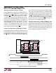
mentation amplifier is used at low gain. If this amplifier is
used at a gain of 10, the gain error is only 10ppm and input
referred noise is reduced to 0.1µV
RMS
. The buffer stages
can also be configured to provide gain of up to 50 with high
gain stability and linearity.
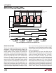
Figure 49 shows an example of a single amplifier used to
produce single-ended gain. This topology is best used in
applications where the gain setting resistor can be made
to match the temperature coefficient of the strain gauges.
If the bridge is composed of precision resistors, with only
one or two variable elements, the reference arm of the
bridge can be made to act in conjunction with the feedback
resistor to determine the gain. If the feedback resistor is
incorporated into the design of the load cell, using resis-
tors which match the temperature coefficient of the load-
cell elements, good results can be achieved without the
need for resistors with a high degree of absolute accuracy.
The common mode voltage in this case, is again a function
of the bridge output. Differential gain as used with a 350Ω
bridge is A
V
= (R1+ R2)/(R1+175Ω). Common mode gain
is half the differential gain. The maximum differential
signal that can be used is 1/4 V
REF
, as opposed to 1/2 V
REF
in the 2-amplifier topology above.
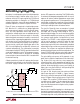
Remote Half Bridge Interface
As opposed to full bridge applications, typical half bridge
applications must contend with nonlinearity in the bridge
output, as signal swing is often much greater. Applications
include RTD’s, thermistors and other resistive elements
that undergo significant changes over their span. For
single variable element bridges, the nonlinearity of the half
bridge output can be eliminated completely; if the refer-
ence arm of the bridge is used as the reference to the ADC,
as shown in Figure 50. The LTC2410 can accept inputs up
to 1/2 V
REF
. Hence, the reference resistor R1 must be at
least 2x the highest value of the variable resistor.
In the case of 100Ω platinum RTD’s, this would suggest a
value of 800Ω for R1. Such a low value for R1 is not
advisable due to self-heating effects. A value of 25.5k is
shown for R1, reducing self-heating effects to acceptable
levels for most sensors.
The basic circuit shown in Figure 50 shows connections
for a full 4-wire connection to the sensor, which may be
located remotely. The differential input connections will
reject induced or coupled 60Hz interference, however, the
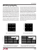
1
Input referred noise for A
V
= 34 for approximately 0.05µV
RMS
, whereas at a gain of 50, it would be
0.048µV
RMS
.
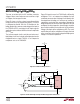
Figure 48. Using Autozero Amplifiers to Reduce Input Referred Noise
0.1µF
8
0.1µF
0.1µF
REF
+
REF
–
SDO
SCK
IN
+
IN
–
CS
GND
V
CC
F
O
312
5V
REF
4
350Ω
BRIDGE
13
5
6
2410 F48
11
1, 7, 8, 9,
10, 15, 16
2
14
LTC2410
RN1 = 5k × 8 RESISTOR ARRAY
U1A, U1B, U2A, U2B = 1/2 LTC1051
–
+
3
2
8
4
U1A
4
5V
+
–
6
5
RN1
1
16
15
2
611
7
1
14
3
710
4
13
89
512
U1B
+
–
2
3
U2A
5V
1
+
–
6
5
U2B
7