
Datasheet


LTC2414/LTC2418
29
241418fa
values for C
REF
will deteriorate the converter offset and
gain performance without significant benefits of reference
filtering and the user is advised to avoid them.
Larger values of reference capacitors (C
REF
> 0.01µF) may
be required as reference filters in certain configurations.
Such capacitors will average the reference sampling charge
and the external source resistance will see a quasi con-
stant reference differential impedance. When F
O
= LOW
(internal oscillator and 60Hz notch), the typical differential
reference resistance is 1.3MΩ which will generate a gain
error of approximately 0.38ppm for each ohm of source
resistance driving REF
+
or REF
–
. When F
O
= HIGH (internal
oscillator and 50Hz notch), the typical differential refer-
ence resistance is 1.56MΩ which will generate a gain error
APPLICATIO S I FOR ATIO
WUUU
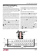
R
SOURCE
(Ω)
1 10 100 1k 10k 100k
+FS ERROR (ppm OF V
REF
)
2414/18 F18
0
–10
–20
–30
–40
–50
V
CC
= 5V
REF
+
= 5V
REF
–
= GND
IN
+
= 3.75V
IN
–
= 1.25V
F
O
= GND
T
A
= 25°C
C
REF
= 0.01µF
C
REF
= 0.001µF
C
REF
= 100pF
C
REF
= 0pF
R
SOURCE
(Ω)
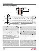
1 10 100 1k 10k 100k
–FS ERROR (ppm OF V
REF
)
2414/18 F19
50
40
30
20
10
0
V
CC
= 5V
REF
+
= 5V
REF
–
= GND
IN
+
= 1.25V
IN
–
= 3.75V
F
O
= GND
T
A
= 25°C
C
REF
= 0.01µF
C
REF
= 0.001µF
C
REF
= 100pF
C
REF
= 0pF
R
SOURCE
(Ω)
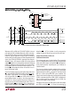
0
100 200 300 400 500 600 700 800 900 1000
+FS ERROR (ppm OF V
REF
)
2414/18 F20
0
–90
–180
–270
–360
–450
V
CC
= 5V
REF
+
= 5V
REF
–
= GND
IN
+
= 3.75V
IN
–
= 1.25V
F
O
= GND
T
A
= 25°C
C
REF
= 0.01µF
C
REF
= 0.1µF
C
REF
= 1µF, 10µF
R
SOURCE
(Ω)
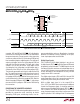
0
100 200 300 400 500 600 700 800 900 1000
–FS ERROR (ppm OF V
REF
)
2414/18 F21
450
360
270
180
90
0
V
CC
= 5V
REF
+
= 5V
REF
–
= GND
IN
+
= 1.25V
IN
–
= 3.75V
F
O
= GND
T
A
= 25°C
C
REF
= 0.01µF
C
REF
= 0.1µF
C
REF
= 1µF, 10µF
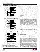
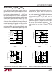
Figure 18. +FS Error vs R
SOURCE
at REF
+
or REF
–
(Small C
IN
)
Figure 19. –FS Error vs R
SOURCE
at REF
+
or REF
–
(Small C
IN
)
Figure 20. +FS Error vs R
SOURCE
at REF
+
and REF
–
(Large C
REF
) Figure 21. –FS Error vs R
SOURCE
at REF
+
and REF
–
(Large C
REF
)
of approximately 0.32ppm for each ohm of source resis-
tance driving REF
+
or REF
–
. When F
O
is driven by an
external oscillator with a frequency f
EOSC
(external conver-
sion clock operation), the typical differential reference
resistance is 0.20 • 10
12
/f
EOSC
Ω and each ohm of source
resistance driving REF
+
or REF
–
will result in
2.47 • 10
–6
• f
EOSC
ppm gain error. The effect of the source
resistance on the two reference pins is additive with
respect to this gain error. The typical +FS and –FS errors
for various combinations of source resistance seen by the
REF
+
and REF
–
pins and external capacitance C
REF
con-
nected to these pins are shown in Figures 18, 19, 20
and 21.