
Datasheet


LTC2414/LTC2418
32
241418fa
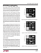
Figure 26. Resolution (Noise
RMS
≤ 1LSB)
vs Output Data Rate and Temperature
Figure 27. Resolution (INL
RMS
≤ 1LSB)
vs Output Data Rate and Temperature
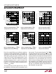
Figure 28. Offset Error vs Output
Data Rate and Reference Voltage
Figure 29. Resolution (Noise
RMS
≤ 1LSB) vs
Output Data Rate and Reference Voltage
Figure 30. Resolution (INL
MAX
≤ 1LSB) vs
Output Data Rate and Reference Voltage
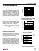
Figure 31. Input Signal Bandwidth
Using the Internal Oscillator
APPLICATIO S I FOR ATIO
WUUU
OUTPUT DATA RATE (READINGS/SEC)
0 102030405060708090100
RESOLUTION (BITS)
2414/18 F26
24
23
22
21
20
19
18
17
16
15
14
13
12
T
A
= 85°C
V
CC
= 5V
REF
+
= 5V
REF
–
= GND
V
INCM
= 2.5V
V
IN
= 0V
SDI = GND
F
O
= EXTERNAL OSCILLATOR
RESOLUTION = LOG
2
(V
REF
/NOISE
RMS
)
T
A
= 25°C
OUTPUT DATA RATE (READINGS/SEC)
0 102030405060708090100
RESOLUTION (BITS)
2414/18 F27
22
20
18
16
14
12
10
8
T
A
= 85°C
V
CC
= 5V
REF
+
= 5V
REF
–
= GND
V
INCM
= 2.5V
–2.5V < V
IN
< 2.5V
SDI = GND
F
O
= EXTERNAL OSCILLATOR
RESOLUTION = LOG
2
(V
REF
/INL
MAX
)
T
A
= 25°C
OUTPUT DATA RATE (READINGS/SEC)
200
150
100
50
0
–50
OFFSET ERROR (ppm of V
REF
)
2414/18 F28
0 102030
40
50
60 70 80 90 100
V
REF
= 5V
V
REF
= 2.5V
F
O
= EXTERNAL OSCILLATOR
V
CC
= 5V
REF
–
= GND
V
IN
= 0V
V
INCM
= 2.5V
SDI = GND
T
A
= 25°C
OUTPUT DATA RATE (READINGS/SEC)
0 102030405060708090100
RESOLUTION (BITS)
2414/18 F29
24
23
22
21
20
19
18
17
16
15
14
13
12
V
REF
= 5V
V
CC
= 5V
REF
–
= GND
V
INCM
= 2.5V
V
IN
= 0V
SDI = GND
F
O
= EXTERNAL OSCILLATOR
T
A
= 25°C
RESOLUTION = LOG
2
(V
REF
/NOISE
RMS
)
V
REF
= 2.5V
OUTPUT DATA RATE (READINGS/SEC)
0 102030405060708090100
RESOLUTION (BITS)
2414/18 F30
22
20
18
16
14
12
10
8
T
A
= 25°C
V
CC
= 5V
REF
–
= GND
V
INCM
= 0.5 • REF
+
–0.5V • V
REF
< V
IN
< 0.5 • V
REF
SDI = GND
F
O
= EXTERNAL OSCILLATOR
V
REF
= 2.5V
V
REF
= 5V
RESOLUTION =
LOG
2
(V
REF
/INL
MAX
)
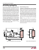
DIFFERENTIAL INPUT SIGNAL FREQUENCY (Hz)
0 0.5 1 1.5 2 2.5 3 3.5 4 4.5 5
INPUT SIGNAL ATTENUATION (dB)
2414/18 F31
0.0
–0.5
–1.0
–1.5
–2.0
–2.5
–3.0
–3.5
–4.0
–4.5
–5.0
–5.5
–6.0
F
O
= HIGH F
O
= LOW
Due to the complex filtering and calibration algorithms
utilized, the converter input bandwidth is not modeled very
accurately by a first order filter with the pole located at the
3dB frequency. When the internal oscillator is used, the
shape of the LTC2414/LTC2418 input bandwidth is shown
in Figure 31 for F
O
= LOW and F
O
= HIGH. When an external
oscillator of frequency f
EOSC
is used, the shape of the
LTC2414/LTC2418 input bandwidth can be derived from
Figure 31, F
O
= LOW curve in which the horizontal axis is
scaled by f
EOSC
/153600.
The conversion noise (1µV
RMS
typical for V
REF
= 5V) can
be modeled by a white noise source connected to a noise
free converter. The noise spectral density is 78nV/√Hz for
an infinite bandwidth source and 107nV/√Hz for a single
0.5MHz pole source. From these numbers, it is clear that
particular attention must be given to the design of external
amplification circuits. Such circuits face the simultaneous
requirements of very low bandwidth (just a few Hz) in
order to reduce the output referred noise and relatively
high bandwidth (at least 500kHz) necessary to drive the
input switched-capacitor network. A possible solution is a
high gain, low bandwidth amplifier stage followed by a
high bandwidth unity-gain buffer.