
Datasheet


LTC2414/LTC2418
37
241418fa
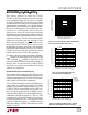
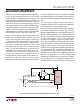
The circuit in Figure 42 shows an example of a simple
amplification scheme. This example produces a differen-
tial output with a common mode voltage of 2.5V, as
determined by the bridge. The use of a true three amplifier
instrumentation amplifier is not necessary, as the LTC2414/
LTC2418 has common mode rejection far beyond that of
most amplifiers. The LTC1051 is a dual autozero amplifier
that can be used to produce a gain of 15 before its input
referred noise dominates the LTC2414/LTC2418 noise.
This example shows a gain of 34, that is determined by a
feedback network built using a resistor array containing 8
individual resistors. The resistors are organized to opti-
mize temperature tracking in the presence of thermal
gradients. The second LTC1051 buffers the low noise
input stage from the transient load steps produced during
conversion.
The gain stability and accuracy of this approach is very
good, due to a statistical improvement in resistor match-
ing. A gain of 34 may seem low, when compared to
common practice in earlier generations of load-cell inter-
faces, however the accuracy of the LTC2414/LTC2418
changes the rationale. Achieving high gain accuracy and
linearity at higher gains may prove difficult, while provid-
ing little benefit in terms of noise reduction.
At a gain of 100, the gain error that could result from
typical open-loop gain of 160dB is –1ppm, however,
worst-case is at the minimum gain of 116dB, giving a gain
error of –158ppm. Worst-case gain error at a gain of 34,
is –54ppm. The use of the LTC1051A reduces the worst-
case gain error to –33ppm. The advantage of gain higher
than 34, then becomes dubious, as the input referred
noise sees little improvement and gain accuracy is poten-
tially compromised.
Note that this 4-amplifier topology has advantages over
the typical integrated 3-amplifier instrumentation ampli-
fier in that it does not have the high noise level common in
the output stage that usually dominates when and instru-
mentation amplifier is used at low gain. If this amplifier is
used at a gain of 10, the gain error is only 10ppm and input
referred noise is reduced to 0.1µV
RMS
. The buffer stages
can also be configured to provide gain of up to 50 with high
gain stability and linearity.
0.1µF
8
0.1µF
0.1µF
REF
+
REF
–
SDI
SCK
SD0
CS
20
18
17
16
CH0
CH1
GND
V
CC
F
O
11
5V
REF
12
350Ω
BRIDGE
21
22
2414/18 F42
15
2
19
LTC2414/
LTC2418
RN1 = 5k × 8 RESISTOR ARRAY
U1A, U1B, U2A, U2B = 1/2 LTC1051
–
+
3
2
8
4
U1A
4
5V
+
–
6
5
RN1
1
16
15
2
611
7
1
14
3
710
4
13
89
512
U1B
+
–
2
3
U2A
5V
1
+
–
6
5
U2B
7
Figure 42. Using Autozero Amplifiers to Reduce Input Referred Noise
APPLICATIO S I FOR ATIO
WUUU