
Datasheet


8
LTC2421/LTC2422
24212f
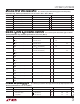
TYPICAL PERFOR A CE CHARACTERISTICS
UW
PIN FUNCTIONS
UUU
V
CC
(Pin 1): Positive Supply Voltage. Bypass to GND
(Pin␣ 6) with a 10µF tantalum capacitor in parallel with
0.1µF ceramic capacitor as close to the part as possible.
FS
SET
(Pin 2): Full-Scale Set Input. This pin defines the
full-scale input value. When V
IN
= FS
SET
, the ADC outputs
full scale (FFFFF
H
). The total reference voltage is
FS
SET
– ZS
SET
.
CH0, CH1 (Pins 4, 3): Analog Input Channels. The input
voltage range is –0.125 • V
REF
to 1.125 • V
REF
. For
V
REF
> 2.5V, the input voltage range may be limited by the
absolute maximum rating of –0.3V to V
CC
+ 0.3V. Conver-
sions are performed alternately between CH0
and CH1 for the LTC2422. Pin 4 is a No Connect (NC) on
the LTC2421.
ZS
SET
(Pin 5): Zero-Scale Set Input. This pin defines the
zero-scale input value. When V
IN
= ZS
SET
, the ADC
outputs zero scale (00000
H
).
GND (Pin 6): Ground. Shared pin for analog ground,
digital ground, reference ground and signal ground. Should
be connected directly to a ground plane through a mini-
mum length trace or it should be the single-point-ground
in a single-point grounding system.
CS (Pin 7): Active LOW Digital Input. A LOW on this pin
enables the SDO digital output and wakes up the ADC.
Following each conversion, the ADC automatically enters
the Sleep mode and remains in this low power state as
long as CS is HIGH. A LOW on CS wakes up the ADC. A
LOW-to-HIGH transition on this pin disables the SDO
digital output. A LOW-to-HIGH transition on CS during the
Data Output transfer aborts the data transfer and starts a
new conversion.
SDO (Pin 8): Three-State Digital Output. During the data
output period, this pin is used for serial data output. When
the chip select CS is HIGH (CS = V
CC
), the SDO pin is in a
high impedance state. During the Conversion and Sleep
periods, this pin can be used as a conversion status out-
put. The conversion status can be observed by pulling CS
LOW.
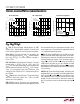
INL vs Output Rate
Resolution vs Output Rate
OUTPUT RATE (Hz)
0
TUE RESOLUTION (BITS)
16
18
20
40
24212 G28
14
12
10
10
20
30
50 60 70 80 90
100
V
CC
= 5V
V
REF
= 5V
F
O
= EXTERNAL
T
A
= –45°C
T
A
= 25°C
T
A
= 90°C
OUTPUT RATE (Hz)
0
TUE RESOLUTION (BITS)
16
18
20
40
24212 G29
14
12
10
10
20
30
50 60 70 80 90
100
V
CC
= 3V
V
REF
= 2.5V
F
O
= EXTERNAL
T
A
= –45°C
T
A
= 25°C
T
A
= 90°C
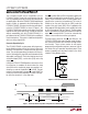
OUTPUT RATE (Hz)
0 7.5
EFFECTIVE RESOLUTION (BITS)
20
22
75
24212 G30
18
16
25
50
100
24
T
A
= 25°C
T
A
= 90°C
T
A
= –45°C
V
CC
= 5V
V
REF
= 5V
f
O
= EXTERNAL
STANDARD DEVIATION
OF 100 SAMPLES
INL vs Output Rate