
Datasheet


LTC2452
8
2452fd
For more information www.linear.com/LTC2452
applicaTions inForMaTion
of magnitude when compared to traditional delta-sigma
architectures. This allows external filter networks to in-
terface directly
to the LTC2452. Since the average input
sampling current is 50nA, an external RC lowpass filter
using 1kΩ and 0.1µF results in <1LSB additional error.
Additionally, there is negligible leakage current between
IN
+
and IN
–
.
Reference Voltage Range
The LTC2453 reference input range is 2.5V to V
CC
. For the
simplest operation, REF can be shorted to V
CC
.
Input Voltage Range
As mentioned in the Output Data Format section, the out
-
put code is given as 32768 • V
IN
/V
REF
+ 32768. For V
IN
≥
V
REF
, the output code is clamped at 65535 (all ones). For
V
IN
≤ –V
REF
, the output code is clamped at 0 (all zeroes).
The LTC2452 includes a proprietary system that can,
typically, digitize each input 8LSB above V
REF
and below
GND, if the differential input is within ±V
REF
. As an ex-
ample (Figure 3), if the
user desires to measure a signal
slightly below ground, the user could set V
IN
–
= GND,
and V
REF
= 5V. If V
IN
+
= GND, the output code would be
approximately 32768. If V
IN
+
= GND – 8LSB = –1.22 mV,
the output code would be approximately 32760.
The total amount of overrange and underrange capability
is
typically 31LSB for a given device. The 31LSB total
is distributed between the overrange and underrange
Figure 3. Output Code vs V
IN
+
with V
IN
–
= 0
capability. For example, if the underrange capability is
8LSB, the overrange capability is typically 31 – 8 = 23LSB.
Output Data Format
The LTC2452 generates a 16-bit direct binary encoded
result. It is provided as a 16-bit serial stream through the
SDO output pin under the control of the SCK input pin
(see Figure 4).
Letting V
IN
= (V
IN
+
– V
IN
–
), the output code is given as
32768 • V
IN
/V
REF
+ 32768. The first bit output by the
LTC2452, D15, is the MSB, which is 1 for V
IN
+
≥ V
IN
–
and
0 for V
IN
+
< V
IN
–
. This bit is followed by successively less
significant bits (D14, D13...) until the LSB is output by the
LTC2452. Table 1 shows some example output codes.
During the data output operation the CS input pin must
be pulled low (CS = LOW). The data output process starts
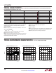
Table 1. LTC2452 Output Data Format
DIFFERENTIAL INPUT
VOLTAGE V
IN
+
– V
IN
–
D15
(MSB)
D14 D13 D12...D2 D1 D0
(LSB)
CORRESPONDING
DECIMAL VALUE
≥V
REF
1 1 1 1 1 1 65535
V
REF
– 1LSB 1 1 1 1 1 0 65534
0.5•V
REF
1 1 0 0 0 0 49152
0.5•V
REF
– 1LSB 1 0 1 1 1 1 49151
0 1 0 0 0 0 0 32768
–1LSB 0 1 1 1 1 1 32767
–0.5•V
REF
0 1 0 0 0 0 16384
–0.5•V
REF
– 1LSB 0 0 1 1 1 1 16383
≤ –V
REF
0 0 0 0 0 0 0
V
IN
+
/V
REF
+
–0.001
OUTPUT CODE
4
12
20
0.001
2452 F03
–4
–12
0
8
16
–8
–16
–20
–0.005
0
0.005
0.0015
SIGNALS
BELOW
GND