
Datasheet


LTC2461/LTC2463
6
24613fa
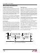
PIN FUNCTIONS
REFOUT (Pin 1): Reference Output Pin. Nominally 1.25V,
this voltage sets the fullscale input range of the ADC. For
noise and reference stability connect to a 0.1µF capacitor
tied to GND. This capacitor value must be less than or
equal to the capacitor tied to the reference compensation
pin (COMP). REFOUT cannot be overdriven by an external
reference. For applications that require an input range
greater than 0V to 1.25V, please refer to the LTC2451/
LTC2453.
COMP (Pin 2): Internal Reference Compensation Pin. For
low noise and reference stability, tie a 0.1μF capacitor to
GND.
A0 (Pin 3): Chip Address Control Pin. The A0 pin can be
tied to GND or V
CC
. If A0 is tied to GND, the LTC2461/
LTC2463 I
2
C address is 0010100. If A0 is tied to V
CC
, the
LTC2461/LTC2463 I
2
C address is 1010100.
GND (Pins 4, 7, 11): Ground. Connect directly to the
ground plane through a low impedance connection.
SCL (Pin 5): Serial Clock Input of the I
2
C Interface. The
LTC2461/LTC2463 can only act as a slave and the SCL pin
only accepts external serial clock. Data is shifted into the
SDA pin on the rising edges of SCL and output through
the SDA pin on the falling edges of SCL.
SDA (Pin 6): Bidirectional Serial Data Line of the I
2
C Inter-
face. The conversion result is output through the SDA pin.
The pin is high impedance unless the LTC2461/LTC2463
is in the data output mode. While the LTC2461/LTC2463
is in the data output mode, SDA is an open drain pull
down (which requires an external 1.7k pull-up resistor
to V
CC
).
REF
–
(Pin 8): Negative Reference Input to the ADC. The
voltage on this pin sets the zero input to the ADC. This
pin should tie directly to ground or the ground sense of
the input sensor.
IN
+
(LTC2463), IN (LTC2461) (Pin 9): Positive input volt-
age for the LTC2463 differential device. ADC input for the
LTC2461 single-ended device.
IN
–
(LTC2463), GND (LTC2461) (Pin 10): Negative input
voltage for the LTC2463 differential device. GND for the
LTC2461 single-ended device.
V
CC
(Pin 12): Positive Supply Voltage. Bypass to GND with
a 10μF capacitor in parallel with a low-series-inductance
0.1μF capacitor located as close to pin 12 as possible.
Exposed Pad (Pin 13 – DFN Package): Ground. Connect
directly to the ground plane through a low impedance
connection.
TYPICAL PERFORMANCE CHARACTERISTICS
(T
A
= 25°C, unless otherwise noted)
Power Supply Rejection
vs Frequency at V
CC
Conversion Time vs Temperature
FREQUENCY AT V
CC
(Hz)
1
REJECTION (dB)
0
24613 G10
–20
–40
–60
–80
–100
–120
10
1k 10k 100k 1M
100
10M
T
A
= 25°C
V
CC
= 4.1V
TEMPERATURE (°C)
–50
CONVERSION TIME (ms)
21
24613 G11
20
16
17
18
19
15
14
–25
25 50 75
0
100
V
CC
= 5V, 4.1V, 3V
V
REF
vs V
CC
2.0 3.52.5 4.03.0 5.0 5.54.5 6.0
V
CC
(V)
V
REF
(V)
1.24892
1.24891
24613 G12
1.24884
1.24885
1.24886
1.24887
1.24888
1.24889
1.24890
T
A
= 25°C