
Datasheet


LTC2482
21
2482fc
APPLICATIONS INFORMATION
An alternate solution is to reduce the edge rate of the control
signals. It should be noted that using very slow edges will
increase the converter power supply current during the
transition time. The differential input architecture reduces
the converter’s sensitivity to ground currents.
Particular attention must be given to the connection of
the f
O
signal when the LTC2482 is used with an external
conversion clock. This clock is active during the conver-
sion time and the normal mode rejection provided by the
internal digital fi lter is not very high at this frequency. A
normal mode signal of this frequency at the converter
reference terminals can result in DC gain and INL errors.
A normal mode signal of this frequency at the converter
input terminals can result in a DC offset error. Such pertur-
bations can occur due to asymmetric capacitive coupling
between the f
O
signal trace and the converter input and/or
reference connection traces. An immediate solution is to
maintain maximum possible separation between the f
O
signal trace and the input/reference signals. When the f
O
signal is parallel terminated near the converter, substantial
AC current is fl owing in the loop formed by the f
O
con-
nection trace, the termination and the ground return path.
Thus, perturbation signals may be inductively coupled into
the converter input and/or reference. In this situation, the
user must reduce to a minimum the loop area for the f
O
signal as well as the loop area for the differential input
and reference connections. Even when f
0
is not driven,
other nearby signals pose similar EMI threats which will
be minimized by following good layout practices.
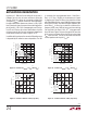
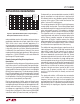
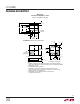
Driving the Input and Reference
The input and reference pins of the LTC2482 converter
are directly connected to a network of sampling capaci-
tors. Depending upon the relation between the differential
input voltage and the differential reference voltage, these
capacitors are switching between these four pins transfer-
ring small amounts of charge in the process. A simplifi ed
equivalent circuit is shown in Figure 10.
For a simple approximation, the source impedance R
S
driving an analog input pin (IN
+
, IN
–
, V
REF
+
or GND) can
be considered to form, together with R
SW
and C
EQ
(see
Figure 10), a fi rst order passive network with a time
constant τ = (R
S
+ R
SW
) • C
EQ
. The converter is able to
sample the input signal with better than 1ppm accuracy
if the sampling period is at least 14 times greater than the
input circuit time constant τ. The sampling process on
the four input analog pins is quasi-independent so each
time constant should be considered by itself and, under
worst-case circumstances, the errors may add.
V
REF
+
V
IN
+
V
CC
R
SW
(TYP)
10k
I
LEAK
I
LEAK
V
CC
I
LEAK
I
LEAK
V
CC
R
SW
(TYP)
10k
C
EQ
12pF
(TYP)
R
SW
(TYP)
10k
I
LEAK
I
IN
+
V
IN
–
I
IN
–
I
REF
+
I
REF
–
2482 F10
I
LEAK
V
CC
I
LEAK
I
LEAK
SWITCHING FREQUENCY
f
SW
= 123kHz INTERNAL OSCILLATOR
f
SW
= 0.4 • f
EOSC
EXTERNAL OSCILLATOR
GND
R
SW
(TYP)
10k
Figure 10. LTC2482 Equivalent Analog Input Current