
Datasheet


LTC2482
25
2482fc
APPLICATIONS INFORMATION
In applications where the reference and input common
mode voltages are different, extra errors are introduced.
For every 1V of the reference and input common mode volt-
age difference (V
REFCM
– V
INCM
) and a 5V reference, each
Ohm of reference source resistance introduces an extra
(V
REFCM
– V
INCM
)/(V
REF
• R
EQ
) full-scale gain error which
is 0.067ppm when using the internal oscillator (50Hz/60Hz
rejection). If an external clock is used, the corresponding
extra gain error is 0.22 • 10
–6
• f
EOSC
ppm.
The magnitude of the dynamic reference current depends
upon the size of the very stable internal sampling capacitors
and upon the accuracy of the converter sampling clock. The
accuracy of the internal clock over the entire temperature
and power supply range is typically better than 0.5%. Such
a specifi cation can also be easily achieved by an external
clock. When relatively stable resistors (50ppm/°C) are
used for the external source impedance seen by V
REF
+
and GND, the expected drift of the dynamic current gain
error will be insignifi cant (about 1% of its value over the
entire temperature and voltage range). Even for the most
stringent applications a one-time calibration operation
may be suffi cient.
In addition to the reference sampling charge, the reference
pins ESD protection diodes have a temperature dependent
leakage current. This leakage current, nominally 1nA
(±10nA max), results in a small gain error. A 100Ω source
resistance will create a 0.05μV typical and 0.5μV maximum
full-scale error.
Output Data Rate
When using its internal oscillator, the LTC2482 produces
6.8ps with a notch frequency of 55Hz, for simultaneous
50Hz/60Hz rejection. The actual output data rate will de-
pend upon the length of the sleep and data output phases
which are controlled by the user and which can be made
insignifi cantly short. When operated with an external
conversion clock (f
O
connected to an external oscillator),
the LTC2482 output data rate can be increased as desired.
The duration of the conversion phase is 41036/f
EOSC
.
An increase in f
EOSC
over the nominal 307.2kHz will
translate into a proportional increase in the maximum
output data rate. The increase in output rate is neverthe-
less accompanied by three potential effects, which must
be carefully considered.
First, a change in f
EOSC
will result in a proportional change
in the internal notch position and in a reduction of the
converter differential mode rejection at the power line fre-
quency. In many applications, the subsequent performance
degradation can be substantially reduced by relying upon
the LTC2482’s exceptional common mode rejection and by
carefully eliminating common mode to differential mode
conversion sources in the input circuit. The user should
avoid single-ended input fi lters and should maintain a
very high degree of matching and symmetry in the circuits
driving the IN
+
and IN
–
pins.
Second, the increase in clock frequency will increase
proportionally the amount of sampling charge transferred
through the input and the reference pins. If large external
input and/or reference capacitors (C
IN
, C
REF
) are used, the
previous section provides formulae for evaluating the effect
of the source resistance upon the converter performance for
any value of f
EOSC
. If small external input and/or reference
capacitors (C
IN
, C
REF
) are used, the effect of the external
source resistance upon the LTC2482 typical performance
can be inferred from Figures 12, 13, 14 and 15 in which
the horizontal axis is scaled by 307200/f
EOSC
.
Third, an increase in the frequency of the external oscillator
above 1MHz (a more than 3× increase in the output data
rate) will start to decrease the effectiveness of the internal
autocalibration circuits. This will result in a progressive
V
IN
/V
REF
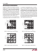
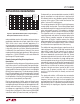
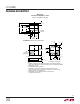
(V)
–0.5
INL (ppm OF V
REF
)
2
6
10
0.3
2482 F18
–2
–6
0
4
8
–4
–8
–10
–0.3
–0.1
0.1
0.5
V
CC
= 5V
V
REF
= 5V
V
IN(CM)
= 2.5V
T
A
= 25°C
C
REF
= 10μF
R = 1k
R = 500Ω
R = 100Ω
Figure 18. INL vs Differential Input Voltage and
Reference Source Resistance for C
REF
> 1μF