
Datasheet


LTC2488
16
2488fa
APPLICATIONS INFORMATION
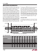
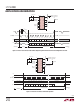
External Serial Clock, Single Cycle Operation
This timing mode uses an external serial clock to shift out
the conversion result and
⎯
C
⎯
S to monitor and control the
state of the conversion cycle (see Figure 4).
The external serial clock mode is selected during the power-
up sequence and on each falling edge of
⎯
C
⎯
S. In order to
enter and remain in the external SCK mode of operation,
SCK must be driven LOW both at power up and on each
⎯
C
⎯
S falling edge. If SCK is HIGH on the falling edge of
⎯
C
⎯
S,
the device will switch to the internal SCK mode.
The serial data output pin (SDO) is Hi-Z as long as
⎯
C
⎯
S is
HIGH. At any time during the conversion cycle,
⎯
C
⎯
S may be
pulled LOW in order to monitor the state of the converter.
While
⎯
C
⎯
S is LOW,
⎯
E
⎯
O
⎯
C is output to the SDO pin.
⎯
E
⎯
O
⎯
C = 1 while a conversion is in progress and
⎯
E
⎯
O
⎯
C = 0 if
the conversion is complete and the device is in the sleep
state. Independent of
⎯
C
⎯
S, the device automatically enters
the sleep state once the conversion is complete; however,
in order to reduce the power,
⎯
C
⎯
S must be HIGH.
When the device is in the sleep state, its conversion re-
sult is held in an internal static shift register. The device
remains in the sleep state until the fi rst rising edge of SCK
is seen while
⎯
C
⎯
S is LOW. The input data is then shifted
in via the SDI pin on each rising edge of SCK (including
the fi rst rising edge). The channel selection will be used
for the following conversion cycle. If the input channel is
changed during this I/O cycle, the new settings take effect
on the conversion cycle following the data input/output
cycle. The output data is shifted out the SDO pin on each
falling edge of SCK. This enables external circuitry to
latch the output on the rising edge of SCK.
⎯
E
⎯
O
⎯
C can be
latched on the fi rst rising edge of SCK and the last bit of
the conversion result can be latched on the 24th rising
edge of SCK. On the 24th falling edge of SCK, the device
begins a new conversion and SDO goes HIGH (
⎯
E
⎯
O
⎯
C = 1)
indicating a conversion is in progress.
At the conclusion of the data cycle,
⎯
C
⎯
S may remain LOW
and
⎯
E
⎯
O
⎯
C monitored as an end-of-conversion interrupt.
Typically,
⎯
C
⎯
S remains LOW during the data output/input
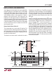
Figure 4. External Serial Clock, Single Cycle Operation
V
CC
F
O
REF
+
REF
–
CH0
CH1
CH2
CH3
COM
SCK
SDI
CS
SDO
GND
12 1
13
14
8
9
10
11
7
3
4
6
5
2
REFERENCE
VOLTAGE
0.1V TO V
CC
ANALOG
INPUTS
= EXTERNAL OSCILLATOR
= INTERNAL OSCILLATOR
LTC2488
2.7V TO 5.5V
0.1μF
10μF
4-WIRE
SPI INTERFACE
Hi-Z
2488 F04
CS
SCK
(EXTERNAL)
SDI
SDO
CONVERSION SLEEP DATA INPUT/OUTPUT CONVERSION
EOC
123456789 192021222324
1 0 EN SGL A2 A1 A0ODD
DON'T CAREDON'T CARE
MSBSIG“0”
LSB
BIT 23 BIT 22 BIT 21 BIT 20 BIT 19 BIT 18 BIT 17 BIT 16 BIT 15 BIT 4 BIT 3 BIT 2 BIT 1 BIT 0