
Datasheet


LTC2495
14
2495fd
cancellation does not interfere with the transparent offset
and full-scale auto-calibration and the absolute accuracy
(full-scale + offset + linearity + drift) is maintained even
with external RC networks.
Power-Up Sequence
The LTC2495 automatically enters an internal reset state
when the power supply voltage, V
CC
, drops below a
threshold of approximately 2.0V. This feature guarantees
the integrity of the conversion result and input channel
selection.
When V
CC
rises above this threshold, the converter creates
an internal power-on-reset (POR) signal with a duration
of approximately 4ms. The POR signal clears all internal
registers. The conversion immediately following a POR
cycle is performed on the input channels IN
+
= CH0 and
IN
–
= CH1 with simultaneous 50Hz/60Hz rejection, 1x
output rate, and gain = 1. The first conversion following a
POR cycle is accurate within the specification of the device
if the power supply voltage is restored to (2.7V to 5.5V)
before the end of the POR interval. A new input channel,
rejection mode, speed mode, temperature selection or
gain can be programmed into the device during this first
data input/output cycle.
Reference Voltage Range
This converter accepts a truly differential external reference
voltage. The absolute/common mode voltage range for the
REF
+
and REF
–
pins covers the entire operating range of
the device (GND to V
CC
). For correct converter operation,
V
REF
must be positive (REF
+
> REF
–
).
The LTC2495 differential reference input range is 0.1V to
V
CC
. For the simplest operation, REF
+
can be shorted to V
CC
and REF
–
can be shorted to GND. The converter output noise
is determined by the thermal noise of the front-end circuits
and, as such, its value in nanovolts is nearly constant with
reference voltage. A decrease in reference voltage will not
significantly improve the converter’s effective resolution.
On the other hand, a decreased reference will improve the
converter’s overall INL performance.
Input Voltage Range
The analog inputs are truly differential with an absolute,
common mode range for the CH0-CH15 and COM input pins
extending from GND – 0.3V to V
CC
+ 0.3V. Outside these
limits, the ESD protection devices begin to turn on and the
errors due to input leakage current increase rapidly. Within
these limits, the LTC2495 converts the bipolar differential
input signal V
IN
= IN
+
– IN
–
(where IN
+
and IN
–
are the
selected input channels), from – FS = – 0.5 • V
REF
/Gain
to + FS = 0.5 • V
REF
/Gain where V
REF
= REF
+
– REF
–
.
Outside this range, the converter indicates the overrange
or the underrange condition using distinct output codes
(see Table 1).
Signals applied to the input (CH0-CH15, COM) may extend
300mV below ground and above V
CC
. In order to limit
any fault current, resistors of up to 5k may be added in
series with the input. The effect of series resistance on
the converter accuracy can be evaluated from the curves
presented in the Input Current/Reference Current sections.
In addition, series resistors will introduce a temperature
dependent error due to input leakage current. A 1nA
input leakage current will develop a 1ppm offset error
on a 5k resistor if V
REF
= 5V. This error has a very strong
temperature dependency.
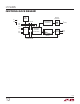
MUXOUT/ADCIN
The outputs of the multiplexer (MUXOUTP/MUXOUTN) and
the inputs to the ADC (ADCINP/ADCINN) can be used to
perform input signal conditioning on any of the selected
input channels or simply shorted together for direct
digitization. If an external amplifier is used, the LTC2495
automatically calibrates both the offset and drift of this
circuit and the Easy Drive sampling scheme enables a
wide variety of amplifiers to be used.
In order to achieve optimum performance, if an external
amplifier is not used, short these pins directly together
(ADCINP to MUXOUTP and ADCINN to MUXOUTN) and
minimize their capacitance to ground.
applications inForMation