
Datasheet
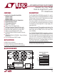
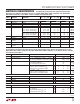
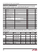

Table Of Contents

LTC2609/LTC2619/LTC2629
3
26091929fb
electrical characteristics
The l denotes the specifications which apply over the full operating
temperature range, otherwise specifications are at T
A
= 25°C. REFA = REFB = REFC = REFD = 4.096V (V
CC
= 5V), REFA = REFB =
REFC = REFD = 2.048V (V
CC
= 2.7V). REFLO = 0V, V
OUT
= unloaded, unless otherwise noted.
SYMBOL PARAMETER CONDITIONS
LTC2629/LTC2629-1 LTC2619/LTC2619-1 LTC2609/LTC2609-1
UNITSMIN TYP MAX MIN TYP MAX MIN TYP MAX
DC Performance
Resolution
l
12 14 16 Bits
Monotonicity (Note 2)
l
12 14 16 Bits
DNL Differential Nonlinearity (Note 2)
l
±0.5 ±1 ±1 LSB
INL Integral Nonlinearity (Note 2)
l
±1 ±4 ±4 ±16 ±16 ±64 LSB
Load Regulation V
REF
= V
CC
= 5V, Mid-Scale
I
OUT
= 0mA to 15mA Sourcing
I
OUT
= 0mA to 15mA Sinking
l
l
0.02
0.02
0.125
0.125
0.1
0.1
0.5
0.5
0.3
0.4
2
2
LSB/mA
LSB/mA
V
REF
= V
CC
= 2.7V, Mid-Scale
I
OUT
= 0mA to 7.5mA Sourcing
I
OUT
= 0mA to 7.5mA Sinking
l
l
0.04
0.05
0.25
0.25
0.2
0.2
1
1
0.7
0.8
4
4
LSB/mA
LSB/mA
ZSE Zero-Scale Error Code = 0
l
1.5 9 1.5 9 1.5 9 mV
V
OS
Offset Error (Note 4)
l
±1 ±9 ±1 ±9 ±1 ±9 mV
V
OS
Temperature
Coefficient
±6 ±6 ±6 µV/°C
GE Gain Error
l
±0.1 ±0.7 ±0.1 ±0.7 ±0.1 ±0.7 %FSR
Gain Temperature
Coefficient
±3 ±3 ±3 ppm/°C
The l denotes the specifications which apply over the full operating temperature range, otherwise specifications are at T
A
= 25°C.
REFA = REFB = REFC = REFD = 4.096V (V
CC
= 5V), REFA = REFB = REFC = REFD = 2.048V (V
CC
= 2.7V). REFLO = 0V, V
OUT
= unloaded,
unless otherwise noted. (Note 9)
SYMBOL PARAMETER CONDITIONS MIN TYP MAX UNITS
PSR Power Supply Rejection V
CC
±10% –80 dB
R
OUT
DC Output Impedance V
REF
= V
CC
= 5V, Mid-Scale; –15mA ≤ I
OUT
≤ 15mA
V
REF
= V
CC
= 2.7V, Mid-Scale; –7.5mA ≤ I
OUT
≤ 7.5mA
l
l
0.030
0.035
0.15
0.15
Ω
Ω
DC Crosstalk (Note 10) Due to Full-Scale Output Change (Note 11)
Due to Load Current Change
Due to Powering Down (Per Channel)
±5
±4
±4
µV
µV/mA
µV
ISC Short-Circuit Output Current V
CC
= 5.5V, V
REF
= 5.5V
Code: Zero-Scale; Forcing Output to V
CC
Code: Full-Scale; Forcing Output to GND
l
l
15
15
36
36
60
60
mA
mA
V
CC
= 2.7V, V
REF
= 2.7V
Code: Zero-Scale; Forcing Output to V
CC
Code: Full-Scale; Forcing Output to GND
l
l
7.5
7.5
22
30
50
50
mA
mA
Reference Input
Input Voltage Range
l
0 V
CC
V
Resistance Normal Mode
l
88 125 160 kΩ
Capacitance 14 pF
I
REF
Reference Current, Power Down Mode DAC Powered Down
l
0.001 1 µA
Power Supply
V
CC
Positive Supply Voltage For Specified Performance
l
2.7 5.5 V
I
CC
Supply Current V
CC
= 5V (Note 3)
V
CC
= 3V (Note 3)
DAC Powered Down (Note 3) V
CC
= 5V
DAC Powered Down (Note 3) V
CC
= 3V
l
l
l
l
1.25
1
0.35
0.15
2
1.6
1
1
mA
mA
µA
µA