
Datasheet
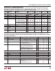
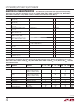

Table Of Contents

LTC2609/LTC2619/LTC2629
4
26091929fb
The l denotes the specifications which apply over the full operating temperature range, otherwise specifications are at T
A
= 25°C.
REFA = REFB = REFC = REFD = 4.096V (V
CC
= 5V), REFA = REFB = REFC = REFD = 2.048V (V
CC
= 2.7V). REFLO = 0V, V
OUT
= unloaded,
unless otherwise noted.
SYMBOL PARAMETER CONDITIONS
LTC2629/LTC2629-1 LTC2619/LTC2619-1 LTC2609/LTC2609-1
UNITSMIN TYP MAX MIN TYP MAX MIN TYP MAX
AC Performance
t
S
Settling Time (Note 5) ±0.024% (±1LSB at 12 Bits)
±0.006% (±1LSB at 14 Bits)
±0.0015% (±1LSB at 16 Bits)
7 7
9
7
9
10
µs
µs
µs
Settling Time for 1LSB Step
(Note 6)
±0.024% (±1LSB at 12 Bits)
±0.006% (±1LSB at 14 Bits)
±0.0015% (±1LSB at 16 Bits)
2.7 2.7
4.8
2.7
4.8
5.2
µs
µs
µs
Voltage Output Slew Rate 0.7 0.7 0.7 V/µs
Capacitive Load Driving 1000 1000 1000 pF
Glitch Impulse At Mid-Scale Transition 12 12 12 nV • s
Multiplying Bandwidth 180 180 180 kHz
e
n
Output Voltage Noise Density At f = 1kHz
At f = 10kHz
120
100
120
100
120
100
nV/√Hz
nV/√Hz
Output Voltage Noise 0.1Hz to 10Hz 15 15 15 µV
P-P
Digital I/O (Note 9)
V
IL
Low Level Input Voltage
(SDA and SCL)
l
0.3V
CC
V
V
IH
High Level Input Voltage
(SDA and SCL)
l
0.7V
CC
V
V
IL(CAn)
Low Level Input Voltage on CAn
(n = 0, 1, 2)
See Test Circuit 1
l
0.15V
CC
V
V
IH(CAn)
High Level Input Voltage on CAn
(n = 0, 1, 2)
See Test Circuit 1
l
0.85V
CC
V
R
INH
Resistance from CAn (n = 0, 1, 2)
to V
CC
to Set CAn = V
CC
See Test Circuit 2
l
10 kΩ
R
INL
Resistance from CAn (n = 0, 1, 2)
to GND to Set CAn = GND
See Test Circuit 2
l
10 kΩ
R
INF
Resistance from CAn (n = 0, 1, 2)
to V
CC
or GND to Set CAn = Float
See Test Circuit 2
l
2 MΩ
V
OL
Low Level Output Voltage Sink Current = 3mA
l
0 0.4 V
t
OF
Output Fall Time V
O
= V
IH(MIN)
to V
O
= V
IL(MAX)
,
C
B
= 10pF to 400pF (Note 7)
l
20 + 0.1C
B
250 ns
t
SP
Pulse Width of Spikes Suppressed by
Input Filter
l
0 50 ns
I
IN
Input Leakage 0.1V
CC
≤ V
IN
≤ 0.9V
CC
l
1 µA
C
IN
I/O Pin Capacitance (Note 12)
l
10 pF
C
B
Capacitive Load for Each Bus Line
l
400 pF
C
CAX
External Capacitive Load on Address
Pins CAn (n = 0, 1, 2)
l
10 pF
electrical characteristics
The l denotes the specifications which apply over the full operating
temperature range, otherwise specifications are at T
A
= 25°C. REFA = REFB = REFC = REFD = 4.096V (V
CC
= 5V), REFA = REFB =
REFC = REFD = 2.048V (V
CC
= 2.7V). REFLO = 0V, V
OUT
= unloaded, unless otherwise noted. (Note 9)