
Datasheet


LTC2600/LTC2610/LTC2620
10
2600fe
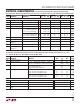
GND (Pin 1/Pin 20): Analog Ground.
V
OUTA
to V
OUTH
(Pins 2-5 and 12-15/Pins 1-48 and
13-16): DAC Analog Voltage Outputs. The output range
is 0 – V
REF
.
REF (Pin 6/Pin 5): Reference Voltage Input. 0V ≤ V
REF
≤ V
CC
.
CS/LD (Pin 7/Pin 7): Serial Interface Chip Select/Load
Input. When CS/LD is low, SCK is enabled for shifting
data on SDI into the register. When CS/LD is taken high,
SCK is disabled and the specifi ed command (see Table 1)
is executed.
SCK (Pin 8/Pin 8): Serial Interface Clock Input. CMOS
and TTL compatible.
SDI (Pin 9/Pin 9): Serial Interface Data Input. Data is ap-
plied to SDI for transfer to the device at the rising edge
of SCK. The LTC2600, LTC2610 and LTC2620 accept input
word lengths of either 24 or 32 bits.
SDO (Pin 10/Pin 10): Serial Interface Data Output. This pin
is used for daisychain operation. The serial output of the
shift register appears at the SDO pin. The data transferred
to the device via the SDI pin is delayed 32 SCK rising
edges before being output at the next falling edge. SDO
is an active output and does not go high impedance, even
when CS/LD is taken to a logic high level.
CLR (Pin 11/Pin 11): Asynchronous Clear Input. A logic
low at this level-triggered input clears all registers and
causes the DAC voltage outputs to drop to 0V. CMOS and
TTL compatible.
V
CC
(Pin 16/Pin 17): Supply Voltage Input. 2.5V ≤ V
CC
≤ 5.5V.
DNC (Pins 6, 12, 18, 19 UFD Only): Do Not Connect.
Exposed Pad (Pin 21 UFD Only): Ground. The exposed
pad must be soldered to the PCB.
PIN FUNCTIONS
(GN/UFD)