
Datasheet


LTC2600/LTC2610/LTC2620
4
2600fe
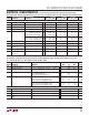
SYMBOL PARAMETER CONDITIONS
LTC2600/LTC2610/LTC2620
UNITSMIN TYP MAX
Power Supply
V
CC
Positive Supply Voltage
l
2.5 5.5 V
I
CC
Supply Current V
CC
= 5V (Note 3)
V
CC
= 3V (Note 3)
All DACs Powered Down (Note 3) V
CC
= 5V
All DACs Powered Down (Note 3) V
CC
= 3V
l
l
l
l
2.6
2.0
0.35
0.10
4
3.2
1
1
mA
mA
μA
μA
Digital I/O
V
IH
Digital Input High Voltage V
CC
= 2.5V to 5.5V
V
CC
= 2.5V to 3.6V
l
l
2.4
2.0
V
V
V
IL
Digital Input Low Voltage V
CC
= 4.5V to 5.5V
V
CC
= 2.5V to 5.5V
l
l
0.8
0.6
V
V
V
OH
Digital Output High Voltage Load Current = –100μA
l
V
CC
– 0.4 V
V
OL
Digital Output Low Voltage Load Current = +100μA
l
0.4 V
I
LK
Digital Input Leakage V
IN
= GND to V
CC
l
±1
μA
C
IN
Digital Input Capacitance (Note 6)
l
8pF
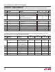
ELECTRICAL CHARACTERISTICS
The l denotes specifi cations which apply over the full operating
temperature range, otherwise specifi cations are at T
A
= 25°C. V
CC
= 2.5V to 5.5V, V
REF
≤ V
CC
, V
OUT
unloaded, unless otherwise noted.
The l denotes specifi cations which apply over the full operating temperature range, otherwise specifi cations are at T
A
= 25°C.
V
CC
= 2.5V to 5.5V, V
REF
≤ V
CC
, V
OUT
unloaded, unless otherwise noted.
SYMBOL PARAMETER CONDITIONS
LTC2620 LTC2610 LTC2600
UNITSMIN TYP MAX MIN TYP MAX MIN TYP MAX
AC Performance
t
S
Settling Time (Note 8)
±0.024% (±1LSB at 12 Bits)
±0.006% (±1LSB at 14 Bits)
±0.0015% (±1LSB at 16 Bits)
77
9
7
9
10
μs
μs
Settling Time for 1LSB Step
(Note 9)
±0.024% (±1LSB at 12 Bits)
±0.006% (±1LSB at 14 Bits)
±0.0015% (±1LSB at 16 Bits)
2.7 2.7
4.8
2.7
4.8
5.2
μs
μs
μs
Voltage Output Slew Rate 0.80 0.80 0.80 V/μs
Capacitive Load Driving 1000 1000 1000 pF
Glitch Impulse At Mid-Scale Transition 12 12 12 nV • s
Multiplying Bandwidth 180 180 180 kHz
e
n
Output Voltage Noise Density At f = 1kHz
At f = 10kHz
120
100
120
100
120
100
nV/√Hz
nV/√Hz
Output Voltage Noise 0.1Hz to 10Hz 15 15 15 μV
P-P