
Datasheet


LTC2630
14
2630ff
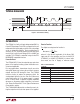
Serial Interface
The CS
/LD input is level triggered. When this input is taken
low, it acts as a chip-select signal, enabling the SDI and
SCK buffers and the input shift register. Data (SDI input)
is transferred at the next 24 rising SCK edges. The 4-bit
command, C3-C0, is loaded first; then 4 don’t-care bits;
and finally the 16-bit data word. The data word comprises
the 12-, 10- or 8-bit input code, ordered MSB-to-LSB, fol-
lowed by 4, 6 or 8 don’t-care bits (LTC2630-12, -10 and
-8 respectively; see Figure 2). Data can only be transferred
to the device when the CS
/LD signal is low, beginning on
the first rising edge of SCK. SCK may be high or low at
the falling edge of CS
/LD. The rising edge of CS/LD ends
the data transfer and causes the device to execute the
command specified in the 24-bit input sequence. The
complete sequence is shown in Figure 3a.
operation
The command (C3-C0) assignments are shown in Table 1.
The first three commands in the table consist of write and
update operations. A Write operation loads a 16-bit data
word from the 24-bit shift register into the input register.
In an Update operation, the input register is copied to the
DAC register and converted to an analog voltage at the
DAC output. Write to and Update combines the first two
commands. The Update operation also powers up the
DAC if it had been in power-down mode. The data path
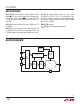
and registers are shown in the Block Diagram.
While the minimum input sequence is 24-bits, it may
optionally be extended to 32-bits to accommodate micro-
processors that have a minimum word width of 16-bits
(2 bytes). To use the 32-bit width, 8 don’t-care bits are
transferred to the device first, followed by the 24-bit se-
quence described. Figure 3b shows the 32-bit sequence.
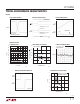
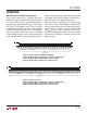
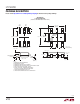
2630 F02
C3
COMMAND 4 DON'T-CARE BITS
MSB
MSB
MSB
LSB
LSB
LSB
DATA (12 BITS + 4 DON'T-CARE BITS)
C2 C1 C0 X X X X D11 D10 D9 D8 D7 D6 D5 D4 D3 D2 D1 D0 X X X X
C3
COMMAND 4 DON'T-CARE BITS DATA (10 BITS + 6 DON'T-CARE BITS)
C2 C1 C0 X X X X D9 D8 D7 D6 D5 D4 D3 D2 D1 D0 X X X X X X
C3
COMMAND
INPUT WORD (LTC2630-12)
INPUT WORD (LTC2630-10)
INPUT WORD (LTC2630-8)
4 DON'T-CARE BITS DATA (8 BITS + 8 DON'T-CARE BITS)
C2 C1 C0 X X X X D7 D6 D5 D4 D3 D2 D1 D0 X X X X X X X X
Figure 2. Command and Data Input Format