
Datasheet


LTC2630
6
2630ff
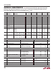
electrical characteristics
SYMBOL PARAMETER CONDITIONS
LTC2630-8 LTC2630-10 LTC2630-12 LTC2630A-12
UNITS
MIN TYP MAX MIN TYP MAX MIN TYP MAX MIN TYP MAX
DC Performance
Resolution
l
8 10 12 12 Bits
Monotonicity V
CC
= 5V, Internal Ref. (Note 4)
l
8 10 12 12 Bits
DNL Differential Nonlinearity V
CC
= 5V, Internal Ref. (Note 4)
l
±0.5 ±0.5 ±1 ±1 LSB
INL Integral Nonlinearity V
CC
= 5V, Internal Ref. (Note 4)
l
±0.05 ±0.5 ±0.2 ±1 ±1 ±2 ±0.5 ±1 LSB
ZSE Zero Scale Error V
CC
= 5V, Internal Ref., Code = 0
l
0.5 5 0.5 5 0.5 5 0.5 5 mV
V
OS
Offset Error V
CC
= 5V, Internal Ref. (Note 5)
l
±0.5 ±5 ±0.5 ±5 ±0.5 ±5 ±0.5 ±5 mV
V
OSTC
V
OS
Temperature
Coefficient
V
CC
= 5V, Internal Ref. (Note 5) ±10 ±10 ±10 ±10 µV/°C
FSE Full Scale Error V
CC
= 5V, Internal Ref.
l
±0.2 ±0.8 ±0.2 ±0.8 ±0.2 ±0.8 ±0.2 ±0.8 %FSR
V
FSTC
Full Scale Voltage
Temperature
Coefficient
V
CC
= 5V, Internal Ref. (Note 10)
C-Grade
I-Grade
H-Grade
±10
±10
±10
±10
±10
±10
±10
±10
±10
±10
±10
±10
ppm/°C
ppm/°C
ppm/°C
Load Regulation V
CC
= 5V ±10%, Internal Ref.,
Mid-Scale, –10mA ≤ I
OUT
≤ 10mA
l
0.006 0.01 0.025 0.04 0.10 0.16 0.10 0.16 LSB/
mA
R
OUT
DC Output Impedance V
CC
= 5V ±10%, Internal Ref.,
Mid-Scale, –10mA ≤ I
OUT
≤ 10mA
l
0.1 0.156 0.1 0.156 0.1 0.156 0.1 0.156 Ω
The l denotes the specifications which apply over the full operating
temperature range, otherwise specifications are at T
A
= 25°C. V
CC
= 4.5V to 5.5V, V
OUT
unloaded unless otherwise specified.
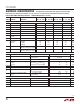
LTC2630-HM12/-HM10/-HM8/-HZ12/-HZ10/-HZ8, LTC2630A-HM12/-HZ12 (V
FS
= 4.096V)
SYMBOL PARAMETER CONDITIONS MIN TYP MAX UNITS
V
OUT
DAC Output Span Supply as Reference
Internal Reference
0V to V
CC
0V to 4.096
V
V
PSR Power Supply Rejection V
CC
= 5V ±10% –80 dB
I
SC
Short Circuit Output Current (Note 6)
Sinking
Sourcing
V
FS
= V
CC
= 5.5V
Zero Scale; V
OUT
Shorted to V
CC
Full Scale; V
OUT
Shorted to GND
l
l
27
–28
50
–50
mA
mA
Power Supply
V
CC
Power Supply Voltage For Specified Performance
l
4.5 5.5 V
I
CC
Supply Current (Note 7) V
CC
= 5V, Supply as Reference
V
CC
= 5V, Internal Reference
l
l
180
200
260
280
µA
µA
I
SD
Supply Current in Power-Down Mode
(Note 7)
V
CC
= 5V, C-Grade, I-Grade
V
CC
= 5V, H-Grade
l
l
0.36
0.36
1.8
5
µA
µA
Digital I/O
V
IH
Digital Input High Voltage
l
2.4 V
V
IL
Digital Input Low Voltage
l
0.8 V
I
LK
Digital Input Leakage V
IN
= GND to V
CC
l
±1 µA
C
IN
Digital Input Capacitance (Note 8)
l
2.5 pF