
Datasheet

LTC2637
16
2637fb
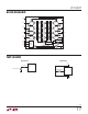
PIN FUNCTIONS
V
CC
(Pin 1/Pin 1): Supply Voltage Input. 2.7V ≤ V
CC
≤ 5.5V
(LTC2637-L) or 4.5V ≤ V
CC
≤ 5.5V (LTC2637-H). Bypass
to GND with a 0.1µF capacitor.
V
OUTA
to V
OUTH
(Pins 2–5, 10–13/Pins 2–5, 12–15): DAC
Analog Voltage Outputs.
CAO (Pin 6/Pin 7): Chip Address Bit 0. Tie this pin to V
CC
,
GND or leave it fl oating to select an I
2
C slave address for
the part (See Tables 1 and 2).
SCL (Pin 7/Pin 8): Serial Clock Input Pin. Data is shifted
into the SDA pin at the rising edges of the clock. This
high impedance pin requires a pull-up resistor or current
source to V
CC
.
SDA (Pin 8/Pin 9): Serial Data Bidirectional Pin. Data is
shifted into the SDA pin and acknowledged by the SDA
pin. This pin is high impedance while data is shifted in.
Open drain N-channel output during acknowledgment. SDA
requires a pull-up resistor or current source to V
CC
.
REF (Pin 9/Pin 11): Reference Voltage Input or Output.
When External Reference mode is selected, REF is an input
(1V ≤ V
REF
≤ V
CC
) where the voltage supplied sets the
full-scale DAC output voltage. When Internal Reference
is selected, the 10ppm/°C 1.25V (LTC2637-L) or 2.048V
(LTC2637-H) internal reference (half full-scale) is available
at the pin. This output may be bypassed to GND with up
to 10µF, and must be buffered when driving external DC
load current.
GND (Pin 14/Pin 16): Ground.
CA2 (Pin 6, MSOP only): Chip Address Bit 2. Tie this pin
to V
CC
, GND or leave it fl oating to select an I
2
C slave ad-
dress for the part (See Table 1).
CA1 (Pin 10, MSOP only): Chip Address Bit 1. Tie this
pin to V
CC
, GND or leave it fl oating to select an I
2
C slave
address for the part (See Table 1).
Exposed Pad (Pin 15, DFN Only): Ground. Must be
soldered to PCB Ground.
(DFN/MSOP)