
Datasheet

LTC2637
20
2637fb
OPERATION
Acknowledge
The Acknowledge (ACK) signal is used for handshaking
between the master and the slave. An ACK (active LOW)
generated by the slave lets the master know that the lat-
est byte of information was properly received. The ACK
related clock pulse is generated by the master. The master
releases the SDA line (HIGH) during the ACK clock pulse.
The slave-receiver must pull down the SDA bus line dur-
ing the ACK clock pulse so that it remains a stable LOW
during the HIGH period of this clock pulse. The LTC2637
responds to a write by a master in this manner but does
not acknowledge a read operation; in that case, SDA is
retained HIGH during the period of the ACK clock pulse.
Chip Address
The state of pins CA0, CA1 and CA2 (CA1 and CA2 are
only available on the MSOP package) determines the slave
address of the part. These pins can each be set to any
one of three states: V
CC
, GND or fl oat. This results in 27
(MSOP Package) or 3 (DFN Package) selectable addresses
for the part. The slave address assignments are shown
in Tables 1 and 2.
In addition to the address selected by the address pins,
the part also responds to a global address. This address
allows a common write to all LTC2637 parts to be ac-
complished using one 3-byte write transaction on the
I
2
C bus. The global address, listed at the end of Tables 1
and 2, is a 7-bit hardwired address not selectable by CA0,
CA1 or CA2. If another global address is required, please
consult the factory.
The maximum capacitive load allowed on the address pins
(CA0, CA1 and CA2) is 10pF, as these pins are driven during
address detection to determine if they are fl oating.
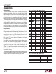
Table 1. Slave Address Map (MSOP Package)
CA2 CA1 CA0 A6 A5 A4 A3 A2 A1 A0
GNDGNDGND0010000
GNDGNDFLOAT0010001
GND GND V
CC
0010010
GNDFLOATGND0010011
GNDFLOATFLOAT0100000
GND FLOAT V
CC
0100001
GND V
CC
GND0100010
GND V
CC
FLOAT0100011
GND V
CC
V
CC
0110000
FLOATGNDGND0110001
FLOATGNDFLOAT0110010
FLOAT GND V
CC
0110011
FLOATFLOATGND1000000
FLOATFLOATFLOAT1000001
FLOAT FLOAT V
CC
1000010
FLOAT V
CC
GND1000011
FLOAT V
CC
FLOAT1010000
FLOAT V
CC
V
CC
1010001
V
CC
GNDGND1010010
V
CC
GNDFLOAT1010011
V
CC
GND V
CC
1100000
V
CC
FLOATGND1100001
V
CC
FLOATFLOAT1100010
V
CC
FLOAT V
CC
1100011
V
CC
V
CC
GND1110000
V
CC
V
CC
FLOAT1110001
V
CC
V
CC
V
CC
1110010
GLOBAL ADDRESS 1110011
Table 2. Slave Address Map (DFN Package)
CA0 A6A5A4A3A2A1A0
GND 0010000
FLOAT 0010001
V
CC
0010010
GLOBAL ADDRESS 1 1 1 0 0 1 1