
Datasheet


LTC2637
24
2637fb
analog section of the ground plane. The resistance from
the LTC2637 GND pin to the ground plane should be as
low as possible. Resistance here will add directly to the
effective DC output impedance of the device (typically
0.1). Note that the LTC2637 is no more susceptible to
this effect than any other parts of this type; on the con-
trary, it allows layout-based performance improvements
to shine rather than limiting attainable performance with
excessive internal resistance.
Another technique for minimizing errors is to use a sepa-
rate power ground return trace on another board layer.
The trace should run between the point where the power
supply is connected to the board and the DAC ground pin.
Thus the DAC ground pin becomes the common point for
analog ground, digital ground, and power ground. When
the LTC2637 is sinking large currents, this current fl ows
out the ground pin and directly to the power ground trace
without affecting the analog ground plane voltage.
It is sometimes necessary to interrupt the ground plane
to confi ne digital ground currents to the digital portion of
the plane. When doing this, make the gap in the plane only
as long as it needs to be to serve its purpose and ensure
that no traces cross over the gap.
OPERATION
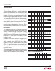
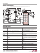
A6 A5 A4 A3 A2 A1 A0 W C3
C3ACK
SLAVE ADDRESS
ACK ACK ACK
C2 C1 C0
A3 A2 A1 A0
D11 D10 D9 D8
D7 D6 D5 D4
D3 D2 D1 D0
XXXX
A6
START STOP
FULL-SCALE
VOLTAGE
ZERO-SCALE
VOLTAGE
SDA
SCL
X = DON’T CARE
V
OUT
A5 A4 A3 A2 A1 A0 C2 C1 C0 A3 A2 A1 A0
8912345
67
12345
67
8912345
67 89123456789
COMMAND/ADDRESS MS DATA LS DATA
2637 F04
Figure 4. Typical LTC2637 Input Waveform—Programming DAC Output for Full-Scale
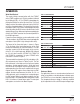
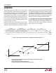
Figure 5. Effects of Rail-to-Rail Operation On a DAC Transfer Curve (Shown for 12 Bits).
(a) Overall Transfer Function
(b) Effect of Negative Offset for Codes Near Zero
(c) Effect of Positive Full-Scale Error for Codes Near Full-Scale
2637 F04
INPUT CODE
(b)
OUTPUT
VOLTAGE
NEGATIVE
OFFSET
0V
0V
2,0480 4,095
INPUT CODE
OUTPUT
VOLTAGE
(a)
V
REF
= V
CC
V
REF
= V
CC
(c)
INPUT CODE
OUTPUT
VOLTAGE
POSITIVE
FSE