
Datasheet


LTC2641/LTC2642
9
26412fc
For more information www.linear.com/LTC2641
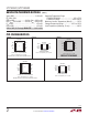
pin FuncTions
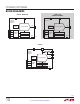
LTC2641 – MSOP, DFN Packages
REF (Pin 1): Reference Voltage Input. Apply an external
reference at REF between 2V and V
DD
.
CS (Pin 2): Serial Interface Chip Select/Load Input. When
CS is low, SCLK is enabled for shifting in data on DIN.
When CS is taken high, SCLK is disabled, the 16-bit input
word is latched and the DAC is updated.
SCLK (Pin 3): Serial Interface Clock Input. CMOS and
TTL compatible.
DIN (Pin 4): Serial Interface Data Input. Data is applied
to DIN for transfer to the device at the rising edge of
SCLK.
CLR (Pin 5): Asynchronous Clear Input. A logic low clears
the DAC to code 0.
V
OUT
(Pin 6): DAC Output Voltage. The output range is
0V to V
REF
.
V
DD
(Pin 7): Supply Voltage. Set between 2.7V and
5.5V.
GND (Pin 8): Circuit Ground.
Exposed Pad (DFN Pin 9): Circuit Ground. Must be sol
-
dered to PCB ground.
LTC2641 – SO Package OBSOLETE
V
OUT
(Pin 1): DAC Output Voltage. The output range is
0V to V
REF
.
GND (Pin 2): Circuit Ground.
REF (Pin 3): Reference Voltage Input. Apply an external
reference at REF between 2V and V
DD
.
CS (Pin 4): Serial Interface Chip Select/Load Input. When
CS is low, SCLK is enabled for shifting in data on DIN.
When CS is taken high, SCLK is disabled, the 16-bit input
word is latched and the DAC is updated.
SCLK (Pin 5): Serial Interface Clock Input. CMOS and
TTL compatible.
DIN (Pin 6): Serial Interface Data Input. Data is applied
to DIN for transfer to the device at the rising edge of
SCLK.
GND (Pin 7): Circuit Ground Pin. Must be connected to
Pin 2 (GND).
V
DD
(Pin 8): Supply Voltage. Set between 2.7V and
5.5V.
LTC2642 – MSOP, DFN Packages
REF (Pin 1): Reference Voltage Input. Apply an external
reference at REF between 2V and V
DD
.
CS (Pin 2): Serial Interface Chip Select/Load Input. When
CS is low, SCLK is enabled for shifting in data on DIN.
When CS is taken high, SCLK is disabled, the 16-bit input
word is latched and the DAC is updated.
SCLK (Pin 3): Serial Interface Clock Input. CMOS and
TTL compatible.
DIN (Pin 4): Serial Interface Data Input. Data is applied
to DIN for transfer to the device at the rising edge of
SCLK.
CLR (Pin 5): Asynchronous Clear Input. A logic low clears
the DAC to midscale.
V
OUT
(Pin 6): DAC Output Voltage. The output range is
0V to V
REF
.
INV (Pin 7): Center Tap of Internal Scaling Resistors. Con-
nect to an external amplifier’s inverting input in bipolar
m
o
de.
R
FB
(Pin 8): Feedback Resistor. Connect to an external
amplifier’s output in bipolar mode. The bipolar output
range is –V
REF
to V
REF
.
V
DD
(Pin 9): Supply Voltage. Set between 2.7V and
5.5V.
GND (Pin 10): Circuit Ground.
Exposed Pad (DFN Pin 11): Circuit Ground. Must be
soldered to PCB ground.