
Datasheet

LTC2801/LTC2802/
LTC2803/LTC2804
4
2801234fe
Note 2: All currents into pins are positive; all voltages are referenced to
GND unless otherwise specified.
Note 3: Guaranteed by other measured parameters and not tested directly.
Note 4: Time from PS ↑
or ON/OFF ↑ until V
DD
≥ 5V and V
EE
≤ –5V.
The l denotes the specifications which apply over the full operating
temperature range, otherwise specifications are at T
A
= 25°C, V
CC
= 1.8V to 5.5V, V
L
= 1.8V to 5.5V, Normal Mode. Typical values are
given for V
CC
= V
L
= 3.3V and T
A
= 25°C, unless otherwise noted.
Note 1: Stresses beyond those listed under Absolute Maximum Ratings
may cause permanent damage to the device. Exposure to any Absolute
Maximum Rating condition for extended periods may affect device
reliability and lifetime.
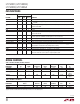
SwitchinG characteriSticS
SYMBOL PARAMETER CONDITIONS MIN TYP MAX UNITS
Maximum Data Rate LTC2801, LTC2803 (Note 3)
R
L
= 3kW, C
L
= 2.5nF
R
L
= 3kW, C
L
= 1nF
l
l
100
250
kbps
kbps
LTC2802, LTC2804 (Note 3)
R
L
= 3kW, C
L
= 2.5nF
R
L
= 3kW, C
L
= 1nF
R
L
= 3kW, C
L
= 250pF
l
l
l
100
250
1000
kbps
kbps
kbps
Driver
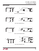
SR(D) Driver Slew Rate LTC2801, LTC2803 (Figure 1)
V
CC
= V
L
= 1.8V, R
L
= 3kW, C
L
= 2.5nF
V
CC
= V
L
= 5.5V, R
L
= 3kW, C
L
= 50pF
l
l
4
30
V/µs
V/µs
LTC2802, LTC2804 (Figure 1)
V
CC
= V
L
= 1.8V, R
L
= 3kW, C
L
= 2.5nF
V
CC
= V
L
= 5.5V, R
L
= 3kW, C
L
= 50pF
l
l
4
150
V/µs
V/µs
t
PHLD
,
t
PLHD
Driver Propagation Delay
R
L
= 3kW, C
L
= 50pF (Figure 2)
LTC2801, LTC2803
LTC2802, L
TC2804
l
l
1
0.2
2
0.5
µs
µs
t
SKEWD
Driver Skew
R
L
= 3kW, C
L
= 50pF (Figure 2)
LTC2801, LTC2803
LTC2802, L
TC2804
100
50
ns
ns
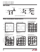
t
PZHD
,
t
PZLD
Driver Output Enable Time
PS = V
L
, MODE = ↑, R
L
= 3kW, C
L
= 50pF
(Figure 4)
l
0.6 2 µs
t
PHZD
,
t
PLZD
Driver Output Disable Time
PS = V
L
, MODE = ↓, R
L
= 3kW, C
L
= 50pF
(Figure 4)
l
0.3 2 µs
Receiver
t
PHLR
, t
PLHR
Receiver Propagation Delay C
L
= 150pF (Figure 3)
l
0.2 0.4 µs
t
SKEWR
Receiver Skew C
L
= 150pF (Figure 3) 50 ns
t
RR
, t
FR
Receiver Rise or Fall Time C
L
= 150pF (Figure 3)
l
60 200 ns
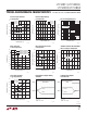
t
PZHR
,
t
PZLR
Shutdown to Receiver Output Enable
PS = MODE = ↑ or ON/OFF = ↑,
R
L
= 1kW, C
L
= 150pF (Figure 5)
l
5 15 µs
t
PHZR
,
t
PLZR
Receiver Output Disable upon Shutdown
PS = MODE = ↓ or ON/OFF = ↓,
R
L
= 1kW, C
L
= 150pF (Figure 5)
l
0.15 0.3 µs
Power Supply Generator
V
DD
/V
EE
Supply Rise Time (Notes 3 and 4)
l
0.2 2 ms