
Datasheet

LTC2801/LTC2802/
LTC2803/LTC2804
10
2801234fe
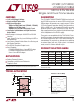
BOOST
REGULATOR
V
EE
V
DD
C3
1µF
C2
1µF
CAP
SW
C1
220nF
L1
10µH
V
CC
C4
1µF
C5
220nF
*OMIT IF V
L
IS CONNECTED TO V
CC
*
V
L
1.8V TO 5.5V
1.8V TO 5.5V
2801 F06
aPPlicationS inForMation
Overview
The LTC2801 family of RS-232 transceivers operates on
a V
CC
supply of 1.8V to 5.5V, utilizing a switching regula-
tor to generate the necessary higher voltage rails for the
drivers. The transceivers interface with logic operating
on any supply from 1.8V to 5.5V, independent of the V
CC
voltage. Depending on the device, one or two control pins
are available to invoke Shutdown, Receiver Active and
Driver Disable features.
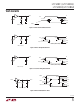
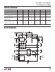
DC-DC Converter
The on-chip DC-DC converter operates from the V
CC
input, generating a 7V V
DD
supply and a charge pumped
– 6.3V V
EE
supply, as shown in Figure 6. V
DD
and V
EE
power the output stage of the drivers and are regulated
to levels that guarantee greater than ±5V output swing.
The DC-DC converter requires a 10µH inductor (L1) and
a bypass capacitor (C4) of at least 1µF. The recommended
size for the charge pump capacitor (C1) is 220nF and for
the storage capacitors (C2 and C3) is 1µF. Larger storage
capacitors up to 4.7µF may be used if C1 is kept at 20% to
50% their size and C4 is also scaled. Locate C1-C4 close
to their associated pins.
Power-Saving Modes
When the DC-DC converter and drivers are turned off (PS
and MODE or ON/OFF = logic low), V
CC
supply current is
reduced to 1µA. Tables 1 and 2 summarize the modes for
each device.
In Shutdown mode, V
L
supply current is reduced to 1µA,
and both receiver and driver outputs assume a high im-
pedance state.
In Receivers Active mode, the quiescent V
L
supply current
is reduced to 15µA and the driver outputs assume a high
impedance state. The receivers operate at a reduced rate
(typically 100 kbps) with hysteresis turned off.
Half-Duplex Operation
When the DC-DC converter is kept on (PS = logic high),
MODE serves as a low-latency driver enable for half-duplex
operation. Each driver is enabled and disabled in less than
2µs, while each receiver remains continuously active. This
mode of operation is illustrated in Figures 15-17.
Battery Operation
To maximize battery life, connect V
CC
(and L1) directly to
the unregulated battery voltage and V
L
to the regulated
supply, as shown in Figure 22. This configuration typically
minimizes conversion loss while providing compatibility
with system logic levels.
Inductor Selection
A 10µH inductor with a saturation current (I
SAT
) rating
of at least 200mA and low DCR (copper wire resistance)
is recommended. Some small inductors meeting these
requirements are listed in Table 3.
Figure 6. DC/DC Converter and Recommended Bypassing
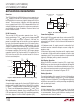
V
L
Logic Supply
A separate logic supply pin V
L
allows the LTC2801 family to
interface with any logic signal from 1.8V to 5.5V, as shown
in Figure 7. Simply connect the desired logic supply to
V
L
. There is no interdependency between V
CC
and V
L
; they
may simultaneously operate at any voltage from 1.8V to
5.5V and sequence in any order. If V
L
is powered separately
from V
CC
, bypass V
L
with a 220nF capacitor (C5).
Figure 7. V
CC
and V
L
Are Independent
ANY VOLTAGE FROM
1.8V TO 5.5V
ANY VOLTAGE FROM
1.8V TO 5.5V
V
L
V
CC
EXTERNAL
DEVICE
RS-232
2801 F07